
1 Foundational Technology Layers
1.1
Process Technology, Equipment, Materials And Manufacturing
Semiconductor process technology, equipment, materials and manufacturing form the base of the ECS value chain producing the chip and packaged chip-level building blocks for all digital applications.
Nano- and microelectronics are key to achieving digital sovereignty in Europe, and they offer a range of solutions for a green and sustainable society. If Europe wants to control the development of a digital future fitted to its citizens and their requirements, as well as its social, economic, industrial and environmental goals, it needs continuous innovation in the field of semiconductor technology.
The key scope of this section is to cover all process technologies, equipment and materials’ research and innovation to enable CMOS compatible semiconductor chip and packaged chip manufacturing inside a cleanroom environment. This includes:
- New materials and engineered substrates to improve device performance,
- process technologies, equipment and manufacturing technology to advance integrated circuit (IC) functionality and/or systems on chips,
- packaging and integration technologies for chips, chiplets, system on a chip (SoC) and system in a package (SiP).
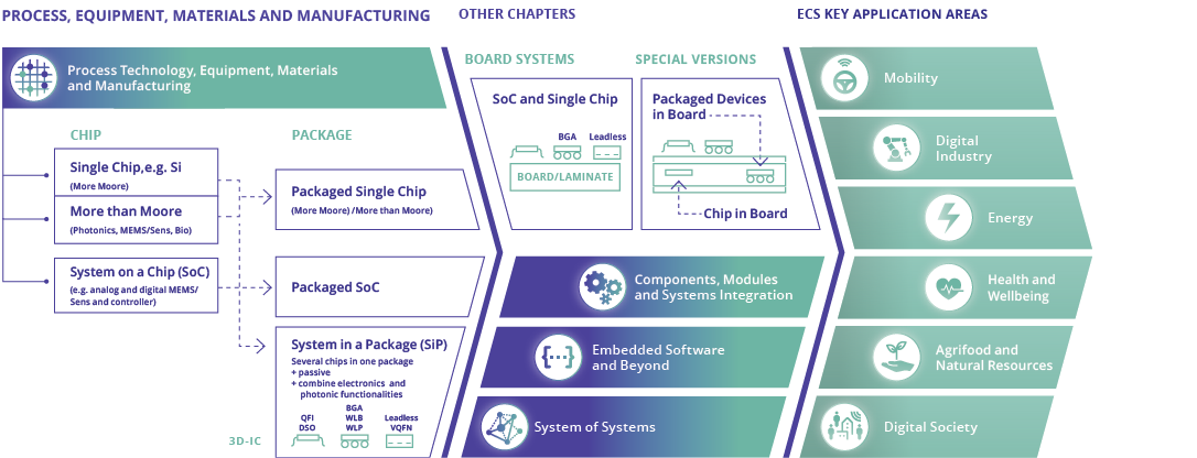
Clearly, the scope of this section involves synergies with other sections in this ECS-SRIA. First and foremost, the section links with Components, Modules and System Integration in Chapter 1.2. In addition, this section also links with Embedded Software and System of Systems (SoS) to allow for an integral system technology co-optimisation approach to deliver application-driven solutions. More details about the synergies with other sections are described in Sub-section 1.1.6. ![]()
Technological challenges arise from evolving and future technologies such as the Internet of Things (IoT), artificial intelligence (AI), edge computing, autonomous driving, high-speed mobile connectivity networks (5G and beyond), image/sound-driven immersive computing (augmented reality) and quantum information processing (QIP). These challenges require advances in: Moore’s law; functional building blocks; ICs; electronics performance; more-than-Moore devices; heterogeneous integration of functionality; and the development of novel computing paradigms and their applicability to “extreme” (e.g. cryogenic or high temperature) environments. Likewise, Industry 4.0 and the sustainable manufacturing of semiconductors require new processes, manufacturing techniques, equipment and materials.
European industry in sectors such as healthcare, automotive, energy, smart cities and manufacturing strongly depends on the timely availability of highly specialised electronics devices enabling added value and new functionalities in their products. Moreover, the advances in chips and packaged chips will strongly contribute to Europe’s ambition to become climate-neutral by 2050, as promoted by the European Green Deal8.
First, across the electronics value chain, the aim is to minimise waste and maximise circular resource usage by extracting the most value from the materials used and repurposing products across their lifecycles. This includes moving towards zero emissions for the direct operation, as well as enhancing the energy efficiency, of electronics manufacturing processes while increasing their productive output.
Second, improving process and manufacturing technologies of semiconductor components, developing new more adequate materials and substrates will allow a more efficient device and system-level use of the energy resources. For instance:
- device scaling by moving into 3D for sub-3 nm node memory and computing technologies will also drive down energy consumption following the power, performance, area and cost (PPAC) scaling roadmaps.
- new embedded non-volatile memory technologies enable local processing and storage of configuration data, decreasing data transmission and energy needs for a wide range of automotive and IoT applications.
- new power electronics devices, either based on silicon or new (GaN, SiC) materials, will increase the energy efficiency of electric powertrains, energy storage, lighting systems, etc.
- improved radio frequency (RF) and Mixed-Signal (MS) device technologies based on new materials such as GaN and IIIV, new switches, and passives enable increased output power and efficiency towards higher frequencies, as well as improved control of the transmission and reception channels with more energy efficiency due to finer RF band control and better directionality.
- new hybrid and heterogeneous combinations between photonic ICs and electronics enable microwave photonic modules – for example, for wideband millimeter-wave processing, and high-bandwidth off-chip and on-chip communications RF filtering.
- new sensor technologies and devices enable better control of processes (e.g. industrial processes, lighting), which contributes to energy saving.
- New sensor and (quantum) information processing units that can operate at and near the theoretical limits allowed by nature.
The main breakthrough enabled by the technological advances discussed in this section concerns the reduction of energy consumption in the various electronic components without any decrease in their performance.
In 2019, the globally consumed power of data centres alone was 200 TWh9, which represents 0.8% of the all power consumed around the world. Investing in more efficient IT hardware including microchips will provide the means to flatten this curve whilst data centre workloads are expected to increase10. Reducing the energy consumption of electronic components is essential for improving the autonomy of electric and hybrid vehicles, the lifetime of battery-powered sensors (for health monitoring, preserving natural resources such as water through more efficient irrigation, etc.), as well as for the development of autonomous sensors with energy harvesters and energy storage.
Since moving data from the logic cores to the adjacent memories is the main contributor to the energy consumption of logic devices (microprocessing units (MPUs), microcontroller units (MCUs), etc.), their conventional von Neumann architecture must be drastically changed in close co-optimisation with other technology innovations. Near-memory or in-memory computing and neuromorphic computing are new architecture paradigms that strongly reduce the movement of data, and accordingly allow decreased overall energy consumption. Specific low- power transistors, memory and 3D-integration technologies need to be developed to ensure close coupling between computer and memory blocks.
The adoption of wide bandgap materials such as GaN and SiC is crucial for allowing higher operating temperatures and reducing the switching losses in power electronics for electric vehicles, as well as to increase their range. GaN/SiC is also important for increasing the power efficiency of 5G RF base stations. In addition, GaN/Si and GaN/SOI can induce the same effect in RF front-end modules when combined with high thermally conductive materials (finite element method, FEM).
New architectures and technologies will be also essential for the future development of 6G communications for improving the bandwidth and data transmission rate, while exhibiting lower latency and lower power consumption.
The exponential increase in internet traffic (which is doubling every 2.5 years9) sets demanding requirements on data communication technologies. Optical interconnects enable higher bandwidth-/ distance products, higher bandwidth density, lower electromagnetic interference, and potentially lower power consumption than electrical interconnects. They are being deployed at increasingly shorter distances – for example, within and between data centres. In the longer term, chip-to-chip and even intra-chip communication may be performed with CMOS-compatible photonics. Beyond these applications, emerging precision applications – including atomic clocks, precision metrology, and transformative applications such as quantum communications and information processing – will also benefit from photonic capabilities integrated with electronics, such as silicon and heterogeneous III/V (membrane) photonics, and potentially disruptive technologies such as nanophotonics and graphene photonics. At the same time, the potential (even remote) of novel computing paradigms such as quantum computing making current security protocols insecure will require development of novel, future proof cryptographic methods.
Other breakthroughs will concern adding intelligence close to the sensors (Intelligence at the edge) and/or to the data sources (IoT), and to integrate the components in a form factor that perfectly suits their applications. The initial generation of “Internet-of-Things” management was cloud-centric, where sensor data were collected from the periphery (or “edge”), then processed and analysed at the enterprise or platform tier. However, in that case, a tremendous amount of data needs to flow to the cloud and back, and a large amount of data processing power is required to structure and analyse it. In such a cloud-focused solution, latency and privacy concerns are often worrisome, or even prohibitive.
The term “embedded AI” or “edge AI” denotes how AI algorithms can be processed locally on a hardware device (e.g. a sensor) close to where the data is generated, and an action may then be required. A device using edge AI can process data it has collected and subsequently take decisions independently, without connecting to a central processing unit (CPU). Where initially local decisions will be supported by inference actions, there will be an evolution to training on the edge devices. Edge AI extends embedded computing, and contributes to economically effective solutions for the societal challenges we are facing in terms of: ![]()
- reducing the energy consumption of the data infrastructure by transmitting only relevant data or pre-treated information (countering the unsustainable explosion of the energy demand by data centres and by telecommunication systems requiring higher bandwidths).
- protecting personal data (GDPR compliance) by local processing and anonymisation of transmitted information.
- increasing security and resilience due to a reduced reliance on telecommunication links as a result of local decision-making.
- reducing latency by reducing the quantity of data needed to be transferred to and from a cloud, which is particularly important for automotive, digital society (real-time control of power distribution, for instance) and manufacturing applications, as well as some health applications.
Rethinking human activities to take advantage of the innovation opportunities offered by hyper-connectivity and AI solution and new kinds of sensors based on miniaturised technologies will create numerous benefits for every new market, ranging from connected cars and digital health to smart home and smart living, and factories of the future. This should include lessons learned from the COVID-19 pandemic like the sudden increase in remote-working.
Sensors and biosensors will be an extensively studied discipline since their rapid, low-cost and highly sensitive features contribute to tremendous advances in many domains. Visible light and IR imagers, lidar, radar and ultrasonic sensors, in combination with high-precision inertial sensors, will be essential for the deployment of advanced driver assistance systems (ADAS). Advancements in chemical-sensing technologies also open the door for multiple new markets. Gas sensors are increasingly integrated into IoT ecosystems to monitor air quality indoors and outdoors – for instance, wearable devices, smart city projects, sensor networks for pollution mapping, smart home electronics and automotive technology. Another key trend to utilise advanced gas-sensing technology is breath analysis, which aims at non-invasive diagnostics via detecting biomarkers from exhaled breath. Furthermore, pressure sensors in human and robot assisted minimally invasive surgery catheters are required to give haptic feedback to the surgeon. Miniaturized ultrasonic sensors open possibilities for minimally invasive medical imaging. However, to access the brain and smaller arteries in the body further miniaturization is required, posing a challenge for current pressure sensor technology.
R&D on highly selective biosensors will contribute to advances in next-generation healthcare, including personalised medicine and the ultrasensitive point-of-care detection of markers for diseases.
Next-generation electronic products are pushing the semiconductor industry to integrate more ultra-thin and flexible ICs. The combination of flexibility and processing capability is very desirable since it reduces weight and enables new form factors, while maintaining desirable functionality such as data logging and RF connectivity. Ultra-thin and flexible ICs enable more efficient and cost-effective solutions that will affect many applications, such as wireless communications, wearable electronics, implantable biomedical devices and the IoT.
The European Chips Act aims to bolster Europe’s competitiveness and resilience in semiconductor technologies and applications, and help achieve both the digital and green transition. Strengthening Europe’s technological leadership in the field is essential to achieve this goal11
Globally, the long-term market trend for electronic components is expected to exceed US $1,000 billion by 203012. In Europe, the semiconductor ecosystem employs some 250,000 people, with 2.5 million in the overall value chain of equipment, materials, semiconductors components, system integration, applications and services – mostly in jobs requiring a high level of education.
In the past, the semiconductor market has been extremely volatile, and R&D investments have been high (up to 10–20% of total revenue). Nonetheless, public/private funding has enabled Europe to lead the world in dedicated semiconductor devices, semiconductor equipment, materials and manufacturing solutions.
Continued investment is vital not only for the ECS industry, but also for the downstream industries that depend on it, including automotive, aviation, space, healthcare, energy, security and telecommunications.
Under Horizon 2020, Future and emerging technologies (FET) flagship initiatives, such as those on graphene and quantum technologies, have been shown to have significant impact on European R&D landscape in these areas. To ensure European leadership in this highly challenging discipline, early involvement of equipment suppliers will bring these activities to the next level in parallel with identifying the best application areas. Importantly, the functionality of several of current ECS technologies needs to be updated to respond to the challenges that new materials and Quantum Information Processing (QIP) are raising. Advanced materials and computational paradigms require not only the development of new scalable platforms, but also non-trivial adaptations and extensions of existing technologies as enablers of such functionalities. For example, any solid state-based quantum computer will need efficient “classical” low-power cryogenic electronics to enable operation of its computing circuit. Both the cryogenic electronics itself (performance, power consumption, noise-compatibility with the fragile qubit layers, 3D integration, packaging...) as the (novel, scalable, efficient) cooling solutions themselves therefore require focused attention.
The creation of manufacturing pilot lines is key, as already demonstrated by successful European projects to date. Pilot lines are a launching ground for new processes, equipment technologies and materials, allowing for early validation of new concepts in support of industrial introduction, and fostering collaboration between industry, research institutes and academia. In addition, they constitute valuable technology platforms for a wide range of applications. Pilot lines are important drivers to advance an understanding of application needs, cut products’ time to market, and showcase European capabilities to potential customers worldwide. Pilot lines provide excellent opportunities for advanced education and training to skilled engineers and scientists. Early availability of innovative semiconductor, sensor and packaging technologies will pave the way to cyber-physical production systems. Having a strong semiconductor portfolio “made in Europe”, with early access for lead system suppliers, is a winning competitive asset for Europe. Such semiconductor manufacturing requires access to advanced materials and characterisation equipment, and competitive manufacturing techniques at the current base of the European value chain. In future, the complete value chain must be covered to promote the competitive situation of the European semiconductor process and integration technology, and to ensure European independence in this field.
Given that in the next decade, 85% of overall global growth is projected to take place outside the EU13, it is essential that strategic industrial ecosystems receive the backing to ensure the robustness that is needed to continue competing globally and to reduce the potential disruptive impact of disasters such as pandemics and climate-related effects. Foreign and domestic investments leveraged by government subsidies have enabled many of these regions to take on a leadership role in several areas of semiconductor manufacturing. Despite competition from East Asia and the US, Europe can reinforce its lead in semiconductor processing and packaging, equipment and smart systems based on the priorities set out in this ECS-SRIA. The first Important Project of Common European Interest (IPCEI) on microelectronics, for example, was a successful step towards strengthening European semiconductor manufacturing in strategic areas where large-scale subsidies in other regions have started to threaten the position of European players. The European Commission has set ambitious targets14 in its ‘Digital Compass’ to double ’cutting-edge semiconductor’ manufacturing in Europe in 2030 – to maintain strategic autonomy, and to be involved in AI and other key technologies of the digital world. In line with this initiative, the EU Chips Act under which a second IPCEI on Microelectronics and Communications Technologies is being set-up to achieve digital leadership in Europe.
Furthermore, through a traditionally strong and advanced educational system, and the presence of world- leading research associations, Europe’s R&D position throughout the whole stack of competencies (also industry-driven) is a unique asset. Continued investment in semiconductor-related studies is crucial to reversing the current trend of declining numbers of students as intended under the Pact for Skills15.
To achieve application breakthroughs and strategic advantage, the European position must be reinforced through leadership in all relevant equipment, materials, processes and manufacturing technologies by driving the following Major Challenges:
- Major Challenge 1: Advanced computing, memory and in-memory computing concepts.
Materials and substrates, process modules and integration technology for novel devices and circuits for advanced computing, memory and in-memory computing concepts based on nano-electronic, photonic or quantum technology. - Major Challenge 2: Novel devices and circuits that enable advanced functionality.
Materials, process modules and integration technology for novel devices and circuits that enable advanced functionality (sensing, actuating, power, connectivity, biomedical, cryogenic operation, etc.). - Major Challenge 3: Advanced heterogeneous integration and packaging solutions.
Advanced heterogeneous integration and packaging solutions for system on a chip (SoC), 2.5 and 3D stacking (including chiplet technology), and smart SiP, sensor integration, photonics, power electronics, and other functionalities required for application domains (such as augmented reality/virtual reality (AR/VR), automotive, (bio)chemical, biomedical, aerospace, etc.). - Major Challenge 4: World-leading and sustainable semiconductor manufacturing equipment and technologies.
World-leading and sustainable semiconductor manufacturing equipment and technologies for the realisation of sub-2 nm node logic and memory according to PPAC roadmap requirements, chips/chiplets with single and/or multi-node layers, advanced functionality devices and heterogeneous integration technology options, as described under Major Challenges 1–3.
1.1.5.1 Major Challenge 1: Advanced computing, memory and in-memory computing concepts
Semiconductor process technology and integration actions will focus on the introduction of new materials, devices and concepts, in close collaboration with the equipment, materials, modelling/simulation and embedded software communities, to allow for the necessary diversity in computing infrastructure. The applications range from high-performance cloud/edge computing in servers, office/home computing, mobile computing, and ultra-low power data processing at the IoT node level up to the highest possible performance.
The obvious solution for transistors with increased electrical performances is the use of fully depleted devices. The industry has adopted two integration methods: FDSOI CMOS and FinFET-style CMOS devices. Chip designers have now embraced the idea that FDSOI and FinFETs can play complementary roles depending on the system requirements (cloud-based services, edge computing or extreme-edge device functionality).
3D FinFET transistors provide high current drive, and hence higher speed, low leakage and, most importantly, less wafer area per transistor than 2D metal–oxide–semiconductor field effect transistor (MOSFET) technology. FinFETs are designed and processed to deliver better performance for applications in high- growth markets such as hyperscale data centres, autonomous vehicles and power-efficient SoCs for the most demanding computer applications. Extreme ultraviolet (EUV) lithography has also made its way into high-volume manufacturing. The international industry value chain is pushing production beyond the 3 nm node by moving towards Gate-All-Around architecture16, and requires solutions in materials and process integration challenges to realise these novel devices. FDSOI is a 2D technology based on a thin buried oxide (BOX) layer under the CMOS channel. FDSOI exhibits several advantages, such as reducing the leakage current at standby mode and its higher tolerance against soft errors compared to traditional structures. FDSOI is perfectly suited for ultra-low-power IoT automotive, edge AI and 5G devices. The leading companies produce 18 nm and 22nm FDSOI-based chips.
A clear differentiation between logic, memory and process information in conventional von Neumann computing schemes necessitates the frequent movement of data between the memory and processor. Thus, much of the execution time and energy consumption is spent in the movement of data, a barrier referred to as the “von Neumann bottleneck”, or “memory wall”. This obstacle has been greatly exacerbated since the advent of data-intensive computing applications, such as AI. Near-memory and in-memory computing are emerging paradigms, wherein the computing system is redesigned to process data at its storage – in the memory – thereby minimising the expensive movement of data.
Near-memory computing involves adding or integrating logic (e.g. accelerators, very small cores, reconfigurable logic) close to or inside the memory. Logic cores are usually placed inside the logic layer of 3D-stacked memories or at the memory controller.
Silicon interposers allow for separate logic chips to be placed in the same die package as a 3D-stacked memory while still taking advantage of the through-silicon via (TSV) bandwidth. Many foundries (Intel, Samsung, TSMC, etc.) offer this kind of heterogeneous integration.
Recent advances in heterogeneous integration technology focus on integrating Si-bridges to connect die together over very short distances along the die perimeter (e.g. Intel EMIB technology, TSMC implementation of Si-bridge and “InFo” technology for the Apple M1 Ultra computer). Currently, several initiatives have been taken by industry groups to attempt to create standards for these “chiplet” interconnect schemes (HBM by JDEC, BOW by OPC , AIB by the “CHIPS” alliance which is further developed to “the Universal Chiplet Interconnect Express”, UCIe).
These heterogeneous integration technologies (Interposers, bridges, chiplets) are often referred to as 2.5D as they still place active die next to each other in a 2D plane. Through 3D integration technology stack active devices vertically on top of each other. This is commonly done in the field of CMOS image sensors and HBM DRAM memory stacks. These 3D integration technologies use TSV technology in the active die, in combination with high density die-to-die or wafer-to-wafer interconnect technologies. This greatly increases the number of functional interconnects per die area on the functional chips. 3D-Interconnect pitch below 10 µm and even down to 1 µm pitch have already been demonstrated.
An even denser 3D interconnect technology could be achieved by so-called “monlithic” 3D integration, a techniqe using sequential manufacturing of multiple layers of active devices and high density (Back-end of line) interconnect layers. Such monolithic integration is not currently available in foundries. In-memory computing also uses the intrinsic properties and operational principles of the memory cells and cell arrays, by inducing interactions between cells such that the cells and or cell arrays can perform computations themselves.
Due to the increasing need for large memory systems by modern applications (big data analytics, AI, etc.), dynamic random access memory (DRAM) and Flash memory scaling is being pushed to its practical limits. It is becoming more difficult to increase the density, reduce the latency and decrease the energy consumption of conventional DRAM and Flash memory architectures. New approaches are therefore being developed to overcome these barriers for implementing near- or in-memory computing. However, it will be difficult to replace DRAM and Flash memory since they are cheap, proven and can handle most tasks.
The first key approach consists of stacking multiple layers of memories (DRAM, Flash). With current manufacturing process technologies, thousands of TSVs can be placed within a single 3D-stacked memory chip. The TSV provide much greater internal memory bandwidth than the narrow memory channel. 3D-stacked DRAM and Flash are also commercially available.
The second major innovation is the use of emerging non-volatile memory (NVM) as parts of the main memory subsystem, and as embedded memories. To avoid DRAM scaling limitations, new memory devices and technologies that can store data at much higher densities than the typical density available in existing DRAM manufacturing process technologies are currently being investigated. The main emerging NVM technologies to augment or replace some DRAM tasks at the main memory layer, and as embedded memories: (i) phase-change memory (PCM); (ii) magnetic RAM or spin-transfer or spin-orbit torque, or voltage-controlled magnetic anisotropy magnetic RAM (MRAM, STT-MRAM, SOT-MRAM, VCMA- MRAM); (iii) metal-oxide resistive RAM (RRAM or ReRAM) and conductive-bridge RAM (CBRAM) or memristors; and (iv) ferroelectric FET (FeFET). All these NVM types are expected to provide memory access latencies and energy usage that are competitive with, or close enough to, DRAM while potentially enabling much larger capacities per chip and non-volatility in main memory.
Driven by market demand on the one hand for advanced high-performance computing devices, and on the other hand for mobility and IoT devices, the advanced Si technology roadmaps for both FinFET and FDSOI will need to be pushed further. To enable this, a wealth of explorations into novel low-thermal-budget-processing 2D materials, nanowires, nanosheets or nanoribbons and quantum dots needs to be combined with significant developments in advanced 3D integration schemes of materials and devices. In parallel, to overcome the von Neumann bottleneck, development of new computing paradigms such as neuromorphic, in-memory and quantum computing is essential. ![]()
New memory concepts will support the correct memory hierarchy in various applications. An example here is the opportunity to push new memory concepts (resistive RAM (RRAM), phase-change RAM (PCRAM), STT- MRAM, FeFET, error correction RAM (EC-RAM)) to the demonstration level in the IoT infrastructure (from server, over edge to nodes). These alternative memories require the development of advanced novel materials (magnetic, phase-change, nanofilament, ferroelectric). A much closer collaboration between device teams and system architects is indispensable in the future. New markets will require storage class memory to bridge the performance gap between DRAM and NAND Flash. IoT applications will require low-power embedded devices and cloud computing with more mass-storage space. The standard memory hierarchy is challenged. Simultaneously, advanced interconnect, SoC integration and packaging issues will need to be addressed (cf. also Major challenges 2 and 3), with innovative solutions to reduce costs being required. The option to use advanced 3D and optical input/output (I/O) technological solutions to circumvent limitations of traditional I/O’s architectures are strengths to foster and build upon in Europe.
To maintain the European competencies in advanced design for integrated circuits and systems, a close link with a strong effort in semiconductor process technology and integration has to be maintained. Issues such as the creation of standards for the IoT, reliability for safety or mission-critical applications, security and privacy requirements need close collaboration among all players to build leadership going forward in this coming generation of advanced and distributed computing infrastructure and diversified system performance.
Expected achievements
Maintaining competence on advanced logic and memory technology in Europe is key to maintaining strategic autonomy and supporting societal benefits from the core technology base. Implementation of dedicated and sustainable pilot lines for specialised logic processes and devices supporting European critical applications is also a major objective, as is the exploration of new devices and architectures for low-power or harsh environment applications.
This challenge includes the following key focus areas:
- Explorations of the scaled Si technology roadmaps of the 3 nm node and beyond (including FDSOI, FinFET/Trigate and stacked gate-all-around horizontal or vertical nanowires, Forksheet, complementary FET architectures, 3D integration), and further device and pitch scaling where parallel conduction paths (nanowires, nanosheets, nanoribbons, etc.) are brought even closer together.
- Exploration and implementation of materials beyond Si (SiGe, SiC, GaN, Ge, InGaAs, InP, functional oxides, 2D material heterostructures, nanowires).
- Novel device, circuit and systems concepts for optimum PPAC specifications, high-energy efficiency and novel paradigms such as for near/in-memory, neuromorphic, optical and quantum computing.
- Long-term challenges such as steep slope switches (tunnel FET, negative capacitance FET, nanoelectromechanical systems, NEMS), spin-based transistors, and alternative high- performance switches.
- Unconventional devices and materials, such as 2D and III-V materials, metamaterials, metasurfaces, nanowires, nanosheets, nanoribbons, nanoparticles, quantum dots, spin effects, functional oxides, ferroelectric and magnetic, which are being investigated to overcome the limits of conventional CMOS logic and memories.
- New embedded non-volatile memory (eNVM) technologies to enable local AI processing and storage of configuration data, which decrease data transmission volume, energy needs and allow for more efficient control of electric powertrains and batteries.
1.1.5.2 Major Challenge 2: Novel devices and circuits that enable advanced functionality
These are materials, process modules and integration technology for novel devices and circuits that enable advanced functionality (sensing, actuating, energy harvesting and storage, connectivity, biomedical, etc.), including wafer or substrate technologies.
This section covers the integration of the logic/memory building blocks (of Major Challenge 1) with other logic/memory building blocks and/or with the non-logic/non-memory building blocks on a single chip (power chips, sensors, NEMS/MEMS (microelectromechanical systems), energy harvesting and storage devices, RF chips such as SiGe or the upcoming GaN and IIIV, passive and active photonic functionalities). The resulting multiple (sub)systems on a chip should enable heterogeneous SiP integration of Major Challenge 3.
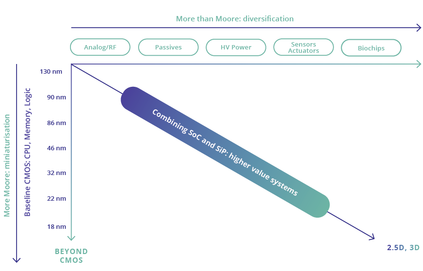
Besides the highly integrated chips necessary to overcome Major Challenge 1 on advanced computing, memory and in-memory computing concepts, many more devices are needed to achieve advanced functionalities – such as sensing and actuating, power management, and interfaces to other systems. This is what has also been named “more than Moore” in recent years, and is an integral part of all systems, as well as one of the strengths of European microelectronics. Given the inherently diverse nature of this sector, the state of the art will be captured by providing a few snapshots of key technologies.
In application-specific logic, the architectures of the embedded NVM implementations are well adapted to current applications, such as flash-based generic or secure micro-controllers, but still lack optimisation to new schemes such as true neuromorphic processors. For IoT applications, logic and RF functions are combined, but not with the highest efficiency required by the ultra-long lifetime. Energy harvesting schemes, often based on photovoltaics, do exist, yet are not always able to provide the requested energy supplement of self-contained low volume and low-cost sensor nodes.
Smart optical, mechanical and magnetic sensors are already able to provide a wealth of information for complex systems. Nevertheless, there are current limits to integrating various types of sensors monolithically. In the field of optical sensors, for instance, depth mapping requires complex scanning schemes using either mechanical systems or large volume and poorly integrated light sources. Devices based on rare or expensive materials, which are not compatible with standard CMOS technology, cover various useful zones of the electromagnetic spectrum. The same is true for chemical-sensing technologies, which are mostly based on metal oxides. While solutions for specific gases and applications are starting to emerge, sensitive and robust technologies using semiconductors still remain to be developed for a large number of applications and species. The situation is similar for many kinds of sensors and actuators. For instance, fine pitch displays are beginning to be possible, but will require new advances both in high brightness low variation sources and assembly methods. ![]()
In power technologies, recent years have seen the emergence of wide bandgap materials able to reduce the losses of power conversion, namely SiC and GaN. These technologies are making quick inroads into the domain of electric and hybrid vehicles. However, they are still nascent, and the challenge is to develop low-cost (involving larger diameter, good quality and less-expensive substrates) and robust technologies. Today, SiC is produced mainly on 150 mm substrates, while GaN has begun to be produced on silicon substrates, but the technology and epitaxy techniques will need further refinement (and even breakthroughs). Moreover, the development of disruptive substrate technologies as well as layer transfer will be key steps toward a cost effective, high performance solution linked with transition from 200 mm to 300 mm substrates which is essential for future integrated logic and power management functions using technologies to combine logic and power transistors. Beside research on wide bandgap materials, the Si-based insulated-gate bipolar transistor (IGBT) technologies have further innovation potential in the area of cost-sensitive applications. Challenges are in the domain of high power and high voltage electronics with high junction temperatures processed on 300 mm substrates – leading to increased power densities and lower costs to support the transformation in the energy systems with Si-based power semiconductors.
For RF and communication technologies, recent advances in integrating RF technologies on low-loss substrates such as SOI have allowed the integration of switches as well as amplifiers on the same silicon substrates. This concept is in production in Europe on 200 mm and 300 mm wafer substrates. Further advances are on the way on 300 mm substrates and technologies, which will allow the integration of more functions and address the requirements of complex 5G systems below and beyond 6 GHz, up to the mm waveband. Synthetic antennae systems for radar or communications are emerging thanks to highly integrated RF technologies, including BiCMOS, but are often limited by power consumption and costs. New, RF technologies delivering high output power and efficiency like RF GaN (GaN-SiC as well as GaN-Si) and IIIV could overcome these limitations. In the field of communications, the integration of photonics technologies with electronics is gaining commercial ground. Further advances in efficient source integration, and modulation and power efficiency, are still needed to use them more widely. New advances in fine photon handling can also open the way to innovative sensing techniques.
In optical communications, the industry trend and needs is to adopt power-efficient, high-speed, silicon photonic links to help addressing the growing demand for data transmission bandwidth, increase computing capabilities and lower consumption. The intrinsic capability of light waves to transmit signals with low latency and power dissipation, at ultrahigh data rates, can be scaled from long-haul infrastructures to intra-datacenter optical links, down to chip-to-chip photonic interconnects. However, bulk silicon cannot meet the necessary requirements of these integrated optics applications which can be addressed with silicon-on-insulator (SOI) technology. SOI photonics will enable in the the development of novel lidar systems as well as support advancements in quantum technologies. By leveraging mature semiconductor manufacturing methods, engineered wafers that incorporate SOI technology offer a powerful approach toward broader adoption of advanced chip-scale integrated optics.
In “traditional” polyimide (PI)-based flexible electronics, the continuing trend is towards more complex designs and large-area processing, especially in displays and sensor arrays. Since the achievement of high-performing flexible electronics by monolithic approaches is limited, hybrid approaches are used when conventional electronics (such as thinned chips) is assembled on flexible electronic substrates. For more complex devices, the reliability and performance of organic materials or mechanical and processing properties of inorganic materials are still a focus of research activities in addition to adapted and optimised assembly techniques. In general, current R&D activities indicate that technical spots can be identified where a merging of novel flexible devices and adapted Si electronics create progress beyond the state of the art.
Depending on the application, the advantages of heterogeneous SoC technology are size, performance, cost, reliability, security and simpler logistics. Therefore, this technology is a key enabler for European industry. To maintain and strengthen Europe’s position, it is necessary to improve existing technologies, and to seamlessly integrate emerging technologies in a reliable and competitive way. All application domains addressed by the ECS SRIA will benefit from components with very diverse functionalities.
Specific process technology platforms may be required, as in the case of biomedical devices for minimally invasive healthcare or point-of-care diagnosis, or mission-critical devices in automotive, avionics and space. Semiconductor process and integration technologies for enabling heterogeneous SoC functionality will focus on the introduction of advanced functional (nano-)materials providing additional functionalities and advanced device concepts.
Innovations for these domains require the exploration and functional integration, preferably in CMOS- compatible processing, of novel materials. A non-exhaustive materials list includes wide bandgap materials, III-V, 2D (e.g. graphene, MoS2 and other transition metal dichalcogenides), 1D (e.g. nanowires, carbon nanotubes) and 0D (e.g. nanoparticles, quantum dots) materials, metal oxides, organic, ferro- and piezoelectric, thermoelectric and magnetic thin films materials, metamaterials and metasurfaces. Obviously, safety and environmental aspects should also be taken into consideration.
The driver for SoC integration is always a clear demand from the application domain. To maintain and push forward Europe’s position, the focus should be on emerging technologies as they are introduced, as well as new developments in the equipment and materials industry, in which Europe has a leading position. Furthermore, the early generation of models and their initial validation for benchmarking and intellectual property (IP) generation are required to reinforce position of Europe in specific design concepts and architecture, especially when used in combination with re-use IP and third-party IP blocks to secure fast time to market.
For structural and flexible electronics, the most important development topics on building the active devices are thinning of Si components for flexibility in heterogenous integration approach, and the development of materials and fabrication methods for flexible active components (e.g. printed transistors). Materials development for active components includes stretchable, printable, conductive and insulative inks. The progress in material science with respect to organic materials, metal oxides, nanomaterials and low-thermal-budget-processing 2D materials will be used for flexible electronic devices to improve their performance. Although there are already many applications that can be addressed by flexible electronics, foldable and stretchable electronics is increasingly on the agenda of research and technology organisations (RTOs) and industry. The objective is to handle electronics like paper or to integrate flexible electronics on 3D-conformable surfaces. The first of these will be important for the display industry, for instance, and the second will be key for the automotive industry as it deals with 3D surfaces in the interior, and integrates electronic functionalities (sensors, displays, lightsources, etc.) on complex surfaces. The requirement on materials and process techniques is much more challenging than for flexible devices since all components and materials have to provide elasticity (intrinsic stretchability).
Expected achievements
This will involve the implementation of pilot lines for integrated application-defined sensors, novel IoT solutions, complex sensor systems and new (bio)medical devices, new RF and mm-wave device options (including radar), photonics options, electronics and packaging solutions. Key will be the initiation of process technology platforms for the exploration and exploitation of advanced functionalities through integration of novel reliable materials.
The exploration and implementation of materials beyond Si will require strategic collaborative EU projects for European industry to become more independent, and will result in the development of a EU-based supply chain for wide-bandgap materials, for example, including a move towards larger substrate sizes of 200 and 300 mm (i.e. SiC and GaN).
Improved materials and assembly techniques will result in more feasible applications for large-area, lightweight, robust and structurally integrated electronics. Hybrid approaches will be used more often, and the boundaries between µ-electronics, semiconductor electronics and flexible electronics will slowly disappear. Strategies to create stretchable electronics will also be developed.
More specifically, the following challenges are identified (this is a non-exhaustive list).
Application-specific logic: as explicitly treated in sub-section 1.1.4.3, heterogeneous SoC integration can require specific solutions for logic to be integrated with more-than-Moore technologies such as the following:
- Tight logic/memory integration for new architectures for neuromorphic computing.
- Logic integration with RF, optical or sensor technologies.
- Ultra-low power (ULP) technology platform and design.
- Integration of lasers and detectors within silicon photonics platform.
Advanced sensor technologies:
- Mechanical sensors (e.g. acceleration, gyroscopes, microphones).
Chemical sensor devices such as selective gas-sensing components for environmental monitoring or smart medicine and smart health (e.g. CO, CO2, NOx, O3, toluene, VOCs, acetone, H2S).
- Physical sensors (magnetic, optical, RF).
- Transmitter/receiver technologies for applications such as lidar and active phased array imaging.
- Biomedical and biochemical sensors.
Advanced power electronics technologies (Si-based, BCD, SiC, GaN, Ga2O3, etc.) to enhance the efficiency of motors, energy storage, lighting systems, etc. More specifically:
- Higher power density and frequency, wide-bandgap materials for high temperature electronics, new CMOS/IGBT processes, integrated logic, uni- and bipolar; high voltage classes, lateral to vertical architectures.
- Materials for energy harvesting (e.g. perovskite solar cells, piezoelectric ceramics and thin films) and storage (e.g. perovskites, ferroelectrics and relaxors), micro-batteries, supercapacitors and wireless power transfer.
- Power devices and modules for highly demanding automotive, industrial and energy infrastructure applications.
- Substrates towards larger diameters to serve future greater demand for cost-sensitive power solutions.
Advanced RF and photonics communication technologies to interface between semiconductors components, subsystems and systems. These technologies should enable better and more energy-efficient control of emission and reception channels (for example, for 5G connectivity and 6G preparations) via:
- New energy-efficient RF and mm-wave integrated device options, including radar (building on e.g. SiGe/BiCMOS, FD SOI, CMOS, GaN, IIIV, PIC).
- Development and characterization of new RF cryogenic electronics for QIP, as well as logic devices at quantum-enabling cryogenic temperatures taking into account the available cooling power of refrigerators and interfacing requirements at different operation temperatures.
- Energy-efficient computing and communication, including a focus on developing new technologies.
- Bringing MOEMS and micro-optics, nanophotonics, optical interconnections, photonics-enabled device and system options into a CMOS-compatible manufacturing and/or packaging flow.
- Integration of solid-state light emitters such as LED and laser with, or onto, a CMOS-compatible platform.
Electronics on flexible and structural substrates are to a large extent dealt with in the Chapter 1.2 on Components, Modules and Systems Integration. However, specific aspects related to process technology are also required:Development of new process capabilities for adapting to flexible, structurally integrated and stretchable electronics, which includes enabling large interconnection areas on substrates.
- Novel (semi)conducting, insulating and encapsulation materials for more reliable devices, and novel substrate materials that can deal with the challenges of flexible electronics.
- Flexible electronics is prone to be used as disposable electronics, and therefore biodegradable materials should be developed that can demonstrate the required performance.
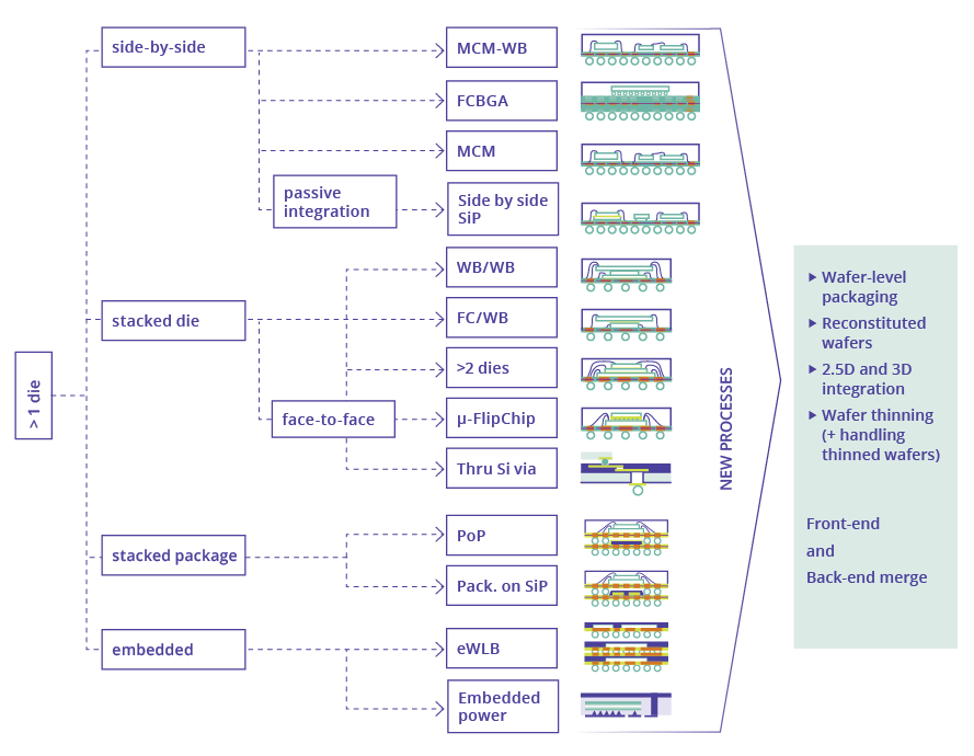
1.1.5.3 Major Challenge 3: Advanced heterogeneous integration and packaging solutions
Advanced heterogeneous integration and packaging solutions for SoC, 2.5 and 3D stacking (including chiplet technology), smart SiP, photonics integration, sensor integration, power electronics, and other functionalities are required for application domains such as AR/VR, automotive, biomedical, avionics, space. Advanced packaging is also required to bridge the scale gap between wafer dies of various technologies and printed circuit boards (PCBs). ![]()
By splitting the packaged chip into smaller functional IP blocks, the overall system yield improves and system performance is enhanced. In addition, by using system-independent IP block design and verification, as well as common die-to-die interfaces (including IP re-use and use of third-party IP), a faster time to market can be achieved.
Over the last few years a huge variety of semiconductor products have emerged where several functions are added in one IC package, enabled by advances in integration and packaging technology.
To maximise the benefits from ICs made for IC-nodes of 7 nm and less, there has already been a move from simple wire bonding to more advanced methods such as ball grid arrays (BGAs), flip chips, wafer-level packaging, fan-out wafer-level packages without substrate interposers and complex 3D structures with TSVs, micro-bumps and thin dies.
The functional diversification of technologies, where digital electronics meets areas such as analogue, photonic and MEMS technologies, has been advanced through the assembly/packaging of heterogeneous elements. For example, in today’s power stages in automotive powertrain applications, there could be power modules that integrate several dies in parallel. Similarly, 5G networks are enabled by advanced RF functionality, often combining a photonic interface with in-package integrated logic and memory functionalities. Upscaling of capacity for photonic ICs may be kickstarted via microwave photonics as a new domain. Semiconductor materials in packaging technology have already moved from being largely silicon-based to more advanced SiC and GaN compounds, as well as towards environmentally friendly lead (Pb) and halogen-free mold compounds. For wire bonding, a similar move from aluminium and gold towards copper and silver wiring has been made. Furthermore, flip chip attach has made a transition to lead-free bumps and BGA using lead-free ball materials.
This challenge covers the integration of new chip technologies in advanced low parasitic packages, as well as chips of different functionalities resulting from the previous two challenges – e.g. CMOS logic, NVM, NEMS/ MEMS, RF, analogue, sensing, actuating, energy harvesting and storage – into a SiP.
Advanced packaging technologies are required for mm-wave applications (> 30 GHz), both GaN/Si RF and high-electron-mobility-transistor (HEMT) devices, or dedicated MEMS and sensor devices (e.g. electro-optics for lidar without moving parts). Depending on the application, heterogeneous SiP technology can provide a better compromise between available functions, performance, cost and time to market.
Assembly and packaging (A&P) technologies, especially those with a focus on system integration, are a key enabler for European industry, including the new field of cryogenic QIP, characterisation of logic devices at quantum-enabling cryogenic temperatures, and associated packaging challenges. To maintain and strengthen Europe’s position, it is necessary to improve existing technologies and develop emerging technologies, as well as to integrate both to advanced electronic systems in a competitive and reliable way. All application domains addressed by the ECS agenda will benefit from innovative assembly and packaging, including SiP components.
Moreover, component carriers also known as Integrated Circuit (IC) Substrates represent a big portion of the package cost (up to 50%), excluding the semiconductor component itself. This is particularly true for Flip Chip Ball Grid Array (FC-BGA) Substrates, which are essential component carriers in high performance computing solutions. Due to the increase of functionality and driven by chiplets integration, FC-BGA substrates are facing many challenges not only in terms of miniaturization, but also they are becoming central elements for power management in advanced computing systems.
Integration of the above functionalities in miniaturised packages and (sub)SiP require fundamental insights into application needs and system architecture. Process and characterisation technology to realise this integration is part of this third Major Challenge, and is essential for ensuring Europe’s prominent role in supplying novel solutions for the various existing and emerging application domains.
Compared to chip technology, assembly and packaging are becoming increasingly important. In many cases, assembly and packaging costs are becoming higher than the chip cost. To reverse this trend, we must focus on dedicated packaging and SiP process technologies that consider all the levels of chip, package and board/ system to identify the optimum trade-offs between function, cost, power, reliability, etc.
To remain economically sustainable and globally competitive, a toolbox must be set up, including evolution of current process technologies as well as new ones, aiming to provide cost-effective and outstanding system integration. Alternative low cost solutions are needed addressing 2.xD integration include interposers based on inorganic, e.g. Si and glass, as well as organic, e.g. FC-BGA and RDL-based, substrates. Furthermore, novel 3D interconnect solutions should be explored enabling new levels of integration for high performance and multifunctional electronic smart systems (ESS).
At the macro-scale level, a system consists of a collection of large functional blocks. These blocks have quite different performance requirements (analogue, high voltage, eNVM, advanced CMOS, fast static RAM (SRAM), multi-sensing capability, etc.) and technology roadmaps. Therefore, for many applications it is of increasing interest to split the system into heterogeneous parts, each realised by optimum technologies at lower cost per function, and assembled with parts using high-density 3D interconnect processes.
It is clear that 3D integration in electronic systems can be realised at different levels of the interconnect hierarchy, each having a different vertical interconnect density. Different technologies are therefore required at different levels of this 3D hierarchy.
Research and development priorities are focused on innovative approaches, such as the following.
Advanced interconnect, encapsulation and packaging technologies:
- Interconnect technologies that allow vertical as well as horizontal integration: this includes process technologies for vertical interconnects, such as TSV, through-encapsulant via (TEV) technologies and microbumps, and copper/copper bonding, as well as process technologies for horizontal interconnects such as thin film technologies for redistribution both on chips and encapsulation materials. A technology base is needed for 3D stacking as well as horizontal interconnecting of dies and chiplets. This also includes interconnects through optical interfaces, most notably off-chip, but also within a package.
- Implementation of advanced nanomaterials and metamaterials, including low-thermal-budget-processing 2D materials, nanowires, nanoparticles and quantum dots with scalable logic and memory device technologies, which will be key for adding new functionalities and developing multifunctional smart systems.
- New materials like Al bumps from Electroplating could solve reliability issues and ensure advanced CMOS compatible packaging on Waferlevel bonding and Chip Integration. Furthermore Power electronic Substrates will benefit from thick Al layers fabricated by novel electroplating technologies Specific power and RF application technologies.
- Solutions for high-frequency miniaturisation, such as for mm-wave applications (> 60 GHz) and for > 100 GHz towards THz applications for which no package solutions currently exist.
- Increasing functionality in IC Substrates for high efficiency power delivery including voltage regulator circuitry and integrated capacitance. Additionally, fine structuring capability achieving high bandwidth interconnections has to be reached either sequentially (2.1D) or recombining separated manufactured carriers (2.3D and 2.5D)
3D integration technologies:
- High-integration density and performance-driven 3D integration (power/speed). For this category, denser 3D integration technologies are required: from the chip I/O-pad level 3D-SIP, to finer grain partitioning of the 3D-SOC and the ultimate transistor-level 3D-IC (see Sub-section 2.3.1 for the 3D landscape).
- Chip-package-board co-design. This will be of utmost importance for introducing innovative products efficiently with a short time to market (and which is closely linked to the work described in Section 2.2).
- System integration partitioning: the choice of 3D interconnect level(s) has a significant impact on system design and the required 3D technology, resulting in a strong interaction need between system design and technology with a significant impact on electronic design automation (EDA) tools.
Enhanced reliability, robustness and sustainability technologies:
- Solutions for high reliability, robustness and high quality. For this, a close consideration of the chip/package interaction, but also of the interaction of chip/package to the board, is required. R&D in this area requires a strong link, especially with materials and their compatibility, and also consideration of the heat dissipation challenges. In addition, variations and extremities in operating environmental conditions should be considered to ensure devices work seamlessly and operational life is not impaired. Avoiding (particle) contamination is another, increasingly critical, requirement. In the last decade nearly all assembly and packaging materials have changed; in the next 10 years, it is expected they will change again. Also, a close link with the Architecture and Design section is crucial here.
- Solutions to test separate components, before and after assembling these in a single package/ subsystem. Concepts like built-in self-test (BIST) and self-repair require some amount of logic integration, and a design providing access for die testing.
System requirements and semiconductor device technology (Major Challenges 1 and 2) will evolve at the same time, creating momentum for further interconnect pitch scaling for 3D integration technology platforms. Hence, the timelines of all four challenges of this section are strongly connected.
1.1.5.4 Major Challenge 4: World-leading and sustainable semiconductor manufacturing equipment and technologies
Semiconductor manufacturing equipment for the high volume production of sub-2 nm node logic and memory according to PPAC roadmap requirements, chips/chiplets with single and/or multi-node layers, advanced functionality devices and heterogeneous integration technology options as described under Major Challenges 1–3.
The semiconductor equipment and manufacturing sector in Europe provides the global market with best- in-class equipment and materials to enable the manufacturing of miniaturised electronic components. The European equipment industry, RTOs and small and medium-sized enterprises (SMEs) active in this sector have a long history of successful mechanical engineering, tailor-made machinery, optical equipment, metrology, inspection and testing equipment, and chemical processing tools. This history of success is prominent in several domains, foremost in lithography (in particular EUV) and metrology, but also in thermal processing, deposition, cleaning and wafer handling, as well as wafer assembly, packaging and in overall product reliability.
At the forefront of semiconductor manufacturing equipment is the production of logic and high-performance memory, which are applied mainly in portable devices as well as advanced cloud computing and data storage facilities. The continuous increase of device density known as Moore’s law is being driven by an ability to create ever-smaller features on wafers. The technology leaps required to keep up with Moore’s law have already been achieved via additional roadmaps complementing ongoing 2D pattern size reductions. They are realised by combining various devices, materials, and 3D and system architecture aspects that required dedicated long-term investment in high-tech equipment solutions. Enabled by current deposition, lithography, etch, processing and metrology tools and their performance, the 5nm technology node is in production by market leaders, solutions for 3nm node has been taped out late 202117, and even Angstrom nodes18 are being explored.
For the production of miniaturised and reliable more-than-Moore electronics components and systems, such as sensors and sensor systems, MEMS, advanced imagers, power electronics devices, automotive electronics, embedded memory devices, mm-wave technologies, and advanced low-power RF technology, many equipment and manufacturing solutions have been implemented. To a large extent, the equipment and manufacturing sector in Europe has developed a full replacement cycle of nearly all assembly and packaging materials by more advanced and sustainable materials over the last decade.
The ever-increasing demand for leading-edge logic and memory technology is driving the development of new equipment and material solutions for sub-2 nm node semiconductor technologies. Besides finding equipment solutions for further shrinking minimum feature sizes well below 10 nm, the alignment accuracy of successive layers, called “overlay” or in another defintition type “Edge Placement Error”, needs to move towards Angstrom levels in a process technology roadmap that combines complex materials in 3D structures and architectures. At the same time, productivity demands on the equipment continue to increase to maintain reduced overall production costs. Process yield also continues to be a challenge with shrinking feature size and the increasing impact of defects and contamination.
The overarching goal of equipment development is to lead the world in miniaturisation techniques by providing appropriate products two years ahead of the shrink roadmap of world’s leading semiconductor device and components manufacturers19. Internationally developed roadmaps such as the International Roadmap for Devices and Systems (IRDS) will also be taken into consideration20. Currently, leading integrated device manufacturers (IDMs) are forecasting a continuation of the technology roadmap following Moore’s law at least until 202921, which corresponds to at least four new generations after the current technology node.
These equipment solutions will enable high-volume manufacturing and fast prototyping of electronic devices in CMOS and beyond CMOS technologies, and therefore allow for supplying the world market with technology-leading, competitive products. Applying new skills and knowhow in areas such as 3D heterogeneous integration and advanced SoC solutions (covered in Major Challenges 2 and 3 of this section) will create and trigger new technological and business opportunities.
For another part of the semiconductor ecosystem, which is also a European strength, system integration equipment is required that can combine chips and wafer technologies of various wafer sizes. In the coming years, 3D integration and SOC manufacturing will add complexity to the global supply chain, and generalise the concept of distributed manufacturing. This will require the development of new concepts for information and control. The interfaces and handovers between wafer technologies and assembly and packaging need to be clearly defined, and will require innovative equipment. Such technologies will necessitate working more closely together, combining front-end wafer equipment, and assembly and packaging equipment. Technologies and methodologies that are well established for Si wafers will partially be reused and adapted for assembly and packaging.
Heterogeneous SoC and SiP integration will pose significant challenges and require R&D activities in a multitude of fields. Equipment and material research must drive the general technology trends in respect to miniaturisation and integration of more functionality into a smaller packaged IC volume, and with higher efficiency, lower power consumption and longer battery life. Processes, equipment and materials for heterogeneous integration can be partially sourced from previous-generation CMOS infrastructures. However, new technology generations will also require capabilities that are not yet available in advanced CMOS fabrication.
Today’s equipment was typically designed for the high-volume continuous production of advanced logic and memory devices, which requires major modifications or re-design when used as production tools for heterogeneous integration. Extending the life of installed equipment to match requirements of this domain via proactive lifecycle management (refurbishment) of these products will provide cost-effective solutions for specific applications. The performance must be enhanced for smaller batch production providing high flexibility and productivity at low cost of ownership.
Furthermore, the trend in solutions of ever-decreasing feature size with an ever-increasing number of features, and interconnects packed onto an IC, puts strong demands on product validation and verification methodologies, as well as on test methodologies and respective equipment.
It is imperative that the equipment and manufacturing sector enables highly flexible, cost-competitive, “green” manufacturing of semiconductor products within the European environment that enables European manufacturers to lead the evolution toward sustainable electronics. To achieve this, semiconductor manufacturing should lead the way in terms of digitisation, with a focus on secure, flexible and sustainable manufacturing and a move from “advanced process control-enabled” equipment to cyber-physical systems. The developed solutions should include innovations for resource-saving and energy-efficiency improvement, with further enhancement of productivity, cycle time, quality and yield performance, at competitive production costs. Furthermore, it will be key to adapt workflows to new, data-driven manufacturing principles adopting digital twins, AI, machine-learning and deep-learning methods, as described in Section 3.3 Digital Industry of this document.
Equipment and equipment integration need to become even smarter than it already is, carrying out intelligent data processing based on enhanced sensors and operating strategies, not only to guarantee stable processes but also to learn, adapt and improve from data gathered and pre-processed in real time.
While the chip advancements are contributing to the industries across verticals, the increased development of chips is also adding to environmental wastes. For instance, fabricating a small 2g microchip (≈ 14-10nm technology node) requires 32-35 kilograms of water, 1.6kg of petroleum and 72g of chemicals22. Since very advanced technology nodes will require more metal layers and lithography steps, and since the chip production could nearly double for satisfying chip demand in the coming years, the environmental impact of the semiconductor industry on power/energy and water consumption, as well as on CO2 and GHG emission will strongly increase up to unacceptable levels to cope with the Green Deal objectives.
Like for its energy consumption, the water and carbon footprints of the semiconductor industry can be classified in three groups or ‘Scopes’:
- Scope 1: Water consumption and CO2 emission as a direct result of the wafer fab usage.
- Scope 2: Water consumption and CO2 emission come from purchased energy powering semiconductor fabs and their associated offices.
- Scope 3: Water consumption and CO2 emission come from all other activities, including the full upstream and downstream supply chain.
A 2011 study23 unveils that the wafer consumption of semiconductor production lines mainly results from the wafer fab usage (Scope 1: 97.3%), while the contributions of scope 2 and 3 were minor: 2.5 and 0.2%, respectively. Each chip needs to be rinsed after many process steps with ultrapure water (UPW) to remove various debris (ions, particles, silica, etc.) from the manufacturing process and prevent the chips from becoming contaminated. It takes 1,400-1,600 litres of municipal water to make 1,000 litres of UPW. Accordingly, for economic rather than ecological reasons, the semiconductor industry has been working for more than twenty years to reduce the amount of water needed to manufacture a chip (Scope 1). To avoid discharges and possible pollution, the proportion of closed-circuit water networks in semiconductor manufacturing plants is increasing. However, the total volume of water consumed by the semiconductor industry has never decreased as the number of chips released from the plants has also exploded over time.
Nowadays, due to the more frequent occurrence of droughts, the water issue is high on the sustainable development plans of major semiconductor companies. Semiconductor manufacturers must focus their efforts on new ways to recycle, reduce, and reuse the water used in their production. Nevertheless new advancements in water treatment must emerge to allow semiconductor manufacturers to recover and reuse wastewater, remove targeted contaminants, and even reclaim valuable products from waste streams.
Indeed, the semiconductor manufacturing process uses a wide range of slurries and chemicals, including hydrofluoric acid for cleaning and etching photosensitive components following the photolithographic process. Other chemicals such as ammonium hydroxide, hydrogen peroxide, hydrochloric acid, sulfuric acid or phosphoric acid are commonly used in rinsing operations. The wastewater includes mixtures of these chemicals, together with other contaminants that result from the manufacturing processes, such as traces of nickel, copper, cobalt, titanium, fluoride, silica, ammonia, and many other organic and inorganic compounds. The complexity of the wafer fabrication processes leads to the generation of wastewater streams that are highly contaminated with chemicals and particles. Successful treatment or reclamation of the waste streams will thus require robust effluent segregation systems, such as micro- or ultra-filtration, reverse osmosis, precipitation, flocculation, sludge and membrane bioreactor. New long-term approaches could deserve some R&D efforts for improving the effluent segregation systems and hence increasing the use of recycled water in semiconductor manufacturing lines.
With about 80% of semiconductor manufacturing emissions falling into either scope 1 or scope 2 categories, fabs control a large portion of their CO2 and Green House Gases (GHG) emission. Scope 2 emissions, which represent the highest proportion of GHG from semiconductor companies, are linked to the energy required to run their production facilities. The sources of these emissions include:
- tool fleets containing hundreds of manufacturing tools, such as lithography equipment, ion implanters, high-temperature furnaces, deposition and etching tools, etc.
- large clean rooms requiring climate and humidity control with overpressure and particle filtration.
- extensive sub-fab facilities for gas abatement, exhaust pumps, water chillers, and water purification.
The energy invested in a completed device can be 5.4 MJ (1.5 kWh) or more per square centimetre24. Furthermore, the fab energy consumption is expected to rise with more advanced process technology nodes.
Compared with “brown” or fossil energy (e.g., coal, gas), “green” energy (e.g., solar, wind, hydropower, and other low carbon) produces up to 30x fewer GHG emissions25. To ensure that sufficient power is always available, fabs often source their electricity from a combination of on-grid and off-grid sources. Most current off-grid power comes from fab-owned fossil fuel power plants. Over the short term, fabs can significantly reduce the energy consumption of these plants by pursuing efficiency improvements by including battery storage or switching to alternative fuels such as biogas or green hydrogen. For on-grid power, fabs may be able to reduce emission by purchasing renewable electricity from utilities through green premium energy offerings, which are often available in Europe.
European semiconductor manufacturing lines must reduce their energy consumption for reducing their operational costs and increasing profitability, but also for decreasing their environmental impact. This can be achieved in the short or midterm by investigating, in collaboration with the equipment suppliers, the energy efficiency of each processing tool and/or by creating energy-efficient process recipes without affecting the overall equipment effectiveness.
Scope 1 emissions, which also significantly add to fab GHG emission profile, arise from process gases used during wafer etching, chamber cleaning, and other tasks. Furthermore, they rise as node size shrinks. These gases, which include PFCs, HFCs, NF3, and N20, have high global-warming potentials. For instance, PFC 14, PFC16, CHF3, NF3 and SF6 respectively exhibit a global warning potential of 6,500x, 9,200x, 11,700x, 17,200x and 23,500x that of CO2. Moreover, the lifetime of such gases in the atmosphere can be very long 50,000 years, 10,000 years and 3,200 years for PFC14, PFC16 and SF6, respectively.
In the short-term, semiconductor companies must collaborate with equipment suppliers to decrease their GHG emission and their operational costs by adjusting process parameters, such as temperature and chamber pressure, cooling water temperatures and by simultaneously optimizing yield and energy consumption during cleaning protocols.
Since much of these GHG and CO2 emissions come from burning perfluorocarbons (PFCs), chemicals, and gases, more efficient gas abatement systems will probably be the main lever to address GHG emissions from process gases over the short to midterm.
Gas recycling of unutilized process gases and by-products through various means, such as membrane separation, cryogenic recovery, adsorption, and desorption can be a long-term approach for reducing the GHG emission. In collaboration with equipment suppliers, semiconductor fab could then refine them into pure process gases that can be used again, potentially reducing process-gas emissions. For this lever to become economically viable, collaboration between semiconductor companies, equipment suppliers and researchers will be compulsory to address these major challenges related to the separation of process-gas outflows and purification.
Another long-term approach could consist in lowering GHG emissions by switching chemicals that have a lower environmental impact than the aforementioned fluoride gases, such as on-site generation of F2 for replacing NF3, since molecular F2 has no global warming potential. Nevertheless, developing new solutions will require strong R&D efforts and will be both costly and time consuming, as is the process for qualifying new chemicals on existing processes and tools.
Since most of the aforementioned fluoride compounds are used for etching, another long-term approach could concern the replacement of some non-critical etching processes by additive manufacturing process steps. Such a replacement will require strong R&D efforts to develop strongly selective deposition processes and/or self-assembled molecules that can prohibit the deposition of metal and dielectrics.
Recycling 1 million cell phones can yield 24kg of gold, 330g of gold, 250kg of silver, 9 kg of palladium, and more than 9,000 kg of copper26. Increase e-waste recycling in order to address the large environmental impact of mining the Earth for metals looks nowadays mandatory. For not wasting mineral resources in view of the limited extractable quantities of metals in the earth’s crust, chipmakers will be more and more concerned with the potential scarcity of some ores that are compulsory for producing ultra-pure metals for the high-volume manufacturing of devices. One way should be to use recycled metals instead of premium metals. Another approach for preventing the use of natural resources consists in recovering the metals for the electronic wastes (e-wastes). Since the amount of precious metal contained in a single smartphone or tablet is weak, and therefore extremely difficult to recover from a scrapped device, the recovery of scarce metals from microelectronic devices opens a wide research domain for material scientists, as well as to ensure sustainable metal sources for chipmakers.
Expected outcome
The goal of the European equipment and manufacturing industry for advanced semiconductor technologies is to lead the world in miniaturisation and performance by supplying new equipment and new materials approximately two years ahead of the introduction schedules for volume production of advanced semiconductor manufacturers. The focus will be on equipment and manufacturing technologies for lithography, metrology and wafer processing, including the respective infrastructure for sub-3 nm node technologies. Further focus needs to be on innovative equipment and material technologies for heterogeneous SoC and SiP integration, enabling advanced packaging of single and/or multi-node chips/chiplets.
Moreover, European semiconductor equipment and manufacturing technologies will be innovation leaders in terms of the use of AI, machine learning in the operation of semiconductor fabrication, and in taking care of limited datasets for model training in a high-mix environment. Solutions for current and future factories will allow high-productivity manufacturing of variable volume, and the energy-efficient, sustainable, resource- saving volume production of semiconductors.
The key focus areas for innovative semiconductor manufacturing equipment technologies are as follows.
Wafer fabrication equipment:
- Advanced patterning equipment for sub-2 nm node wafer processing using deep ultraviolet (DUV) and EUV lithography, and corresponding subsystems and infrastructure (e.g. pellicles, masks and resist).
- Mask manufacturing equipment for sub-2 nm node mask patterning and tuning, defect inspection and repair, metrology and cleaning.
- Advanced holistic lithography using DUV, EUV and next-generation lithography techniques, such as e-beam and mask-less lithography, directed self-assembly (DSA) and nano-imprinting.
- Multi-dimensional metrology (MDM) and inspection for sub-3 nm node devices that combine a all the spectrum of physical tools and data processing techniques.
- Thin film processes including thin film and atomic layer deposition, doping and material modification, and corresponding equipment and materials.
- “Bottom up” technologies to selectively deposit materials on topography or on a selected material.
- Equipment and manufacturing technology for wet and dry processing, wet and dry etching, including (atomic layer) selective etch processing, thermal treatment, laser annealing and wafer preparation.
- Technologies and tools for the manufacturing and integration of semiconductor components made with advanced nanomaterials and metamaterials (low-thermal-budget-processing 2D materials, nanowires, nanoparticles, quantum dots, etc.) with logic and memory technologies.
- High-volume manufacturing tools for the production of III-V, GaN, SiC or other exotic material substrates of up to 200 mm, or 300 mm in the future.
- Dedicated equipment for manufacturing of electronics on flexible, structural and/or bio- compatible substrates.
- New electroplating equipment for ionic liquids (i.e. for Al deposition).
Assembly equipment:
- Equipment and manufacturing technology supporting 3D integration and interconnect capabilities such as chip-to-wafer stacking, fan-out WLP, multi-die packaging, “2.5D” interposers, wafer-to-wafer sequential processing, TSVs and transistor stacking.
- Enhanced equipment optimised for high-volume manufacturing of large batches of the same package into efficient reconfigurable equipment for the manufacturing of different packages in smaller batches.
- New process tools for die separation, attachment, thinning, handling and encapsulation for reliable heterogeneous integration on chip and in package, as well as assembly and packaging of electronics on flexible substrates.
- Equipment development to suit the requirements of multi-component assembly on flexible and stretchable substrates, especially in roll-to-roll for both conductive adhesives and soldering.
- New selective bonding equipment based on inductive or reactive heating.
Test equipment:
- In-line and off-line technologies for the testing, validation and verification (TV&V) of heterogeneous chips and SiP with ever-increasing number of features and ever-decreasing feature size to tackle the challenge of failure localisation in these highly complex (packaged) chips.
- Characterisation equipment for quality control at multiple levels and different scales of semiconductor structures, films and components.
In addition, specific manufacturing technologies are required to enable IC-fabs with interconnected tools to support flexible, sustainable, agile and competitive high-volume semiconductor manufacturing of high- quality, advanced functionality devices and heterogeneous integration technology options in Europe. This leads to the following key focus areas: ![]()
- Enable flexible line management for high-mix and distributed manufacturing lines, including lines for fabrication and deposition of advanced functional (nano) materials.
- Enhance equipment optimised for high-volume manufacturing of large batches of the same chip into efficient reconfigurable equipment for the manufacturing of different chips in smaller batches.
- Enable productivity enhancements (e.g. wafer diameter conversions) for heterogeneous integration technologies to significantly improve cost-competitiveness.
- New manufacturing techniques combining chip and packaging technologies (e.g. chip embedding) will also require new manufacturing logistics and technologies (e.g. panel moulding).
- Adopt factory integration and control systems to address the digital industry challenge of the ECS-SRIA, and to apply fast (and deep) learning as well as semi-automated AI-based decision- making to control processes, to enhance quality, increase reliability, shorten time to stable yield, and preserve knowledge and master complexity in these innovative machine-to-machine domains.
- Apply PAD approaches with a focus on predictive maintenance, virtual metrology, factory simulation and scheduling, wafer-handling automation and the digitisation of the value chain for AI-based decision management. In addition, attention should be given to control system architecture based on machine learning: viz. predictive yield modelling, and holistic risk and decision-mastering (integrate control methods and tools and knowledge systems).
- Doubling semiconductor manufacturing in Europe in 2030 also means evolving and upgrading installed base through incremental approaches, which will necessary mean increased complexity. Managing such hybrid factories will require advanced decision support and diagnosis techniques leveraging IA but also integrating existing human knowledge and know how.
- Develop comprehensive modelling and sharing techniques to enable seamless flow and utilization of information across the whole value chain will require significant evolution of the existing knowledge management techniques and technologies (NLP to exploit existing documentation, diffusion and sharing of cutting-edge or strategic knowledge).
- Future innovations should also address new environmentally friendly solutions for manufacturing (e.g. in terms of energy consumption, chemical usage) and environmentally friendly new materials (e.g. in terms of quality, functionality, defects) in parallel with addressing the continued cost of ownership challenges. This will entail, for example, new precursors, chemicals for deposition and other wafer-processing materials, as well as gas delivery, gas handling, pumps and abatement systems.
To develop these future technologies, it will be key to develop dedicated equipment and manufacturing technologies for the production and characterisation of advanced integrated photonics, as well as for the production of quantum computing chips: ![]()
- In parallel with the new manufacturing/equipment technologies to suit the specific needs of integrated photonics, novel characterisation equipment and methodologies will need to be developed. These may be partly based on available technologies from electronic chip manufacturing and packaging. In addition, completely new and innovative techniques are required. Nanophotonic technologies for enhanced light–matter interaction will require the development of multi-scale fabrication and characterisation techniques suitable for dimensions ranging from a few nanometres to several centimetres. Specific equipment and processes need to be developed to enable industrial-scale fabrication of photonic ICs, such as DUV lithography and epitaxial growth of III-Vs. The hybrid combination of chips from different platforms and technology areas will also be essential to further increase functionality in the modules, and cost- effective volume packaging should therefore be a priority.
- The development of quantum computing technology will require new types of equipment, materials and manufacturing technologies. Advanced implementation options for QIP (superconducting circuits, Majorana states, etc.) often require cryogenic environments and processing. Advanced industrial characterisation equipment tailored to operating in highly challenging environments will be key enablers for such developments to reach market applications. This includes new metrology equipment for mapping electrical and magnetic properties with high spatial and temporal resolution.
All leading European industry and research actors should align their activities with international roadmaps and timelines. Roadmap exercises are being conducted in various projects and communities, including NEREID27 and the IEEE’s IRDS28, in which European academia, RTOs and industry are participating. For system integration, the International Electronics Manufacturing Initiative (iNEMI)29 and the new Heterogeneous Integration Roadmap activities are also considered. The European R&D priorities are planned in synchronisation with global timeframes and developments that are under continuous adaptation. The timelines below are high-level derivatives from these global evolutions, and follow the structure of the four Major Challenges described above.
For Major Challenge 1, the roadmap for process technology and device/system integration presents relatively clear timelines, although economic factors will determine the speed of adoption in industrial manufacturing. Dedicated process technologies (e.g. low-power and high-operating temperature) will follow feature scaling with some delay, focusing on other performance indicators. Areas where the roadmaps and timelines are less clear (e.g. new computing paradigms) will be introduced at low technology readiness levels (TRLs).
For Major Challenges 2 and 3, the timeline of the implementation of new technologies largely depends on the needs and roadmaps of the systems, and will result from the interaction within application-driven projects and test-bed initiatives. The timing of new equipment and manufacturing solutions for these challenges should be derived from the schedules of the major European semiconductor manufacturers. This includes roadmaps for key future semiconductor domains, such as automotive, healthcare, safety and security, power, MEMS, image sensors, biochips, organ-on-a-chip, photonics, lighting, etc. Fast implementation and modification of these new device technologies will pave the way for the technologies of tomorrow.
First, the development of sub-2 nm solutions in terms of equipment and materials as part of Major Challenge 4 needs to be two-to-three years ahead of mass adoption, and is of critical importance to maintaining European leadership. Second, new equipment and materials solutions should be developed in line with the needs defined in the roadmaps of Major Challenges 1–3. Lastly, improving manufacturing efficiency and enhancing yield and reliability are ongoing tasks that need to be performed in accordance with the needs of the “more-Moore” and “more-than-Moore” domains. Fundamentals of “manufacturing science” will concern projects at rather low TRLs (typically 3–5), whereas implementation in pilot lines and full-scale manufacturing lines will contemplate higher TRL projects (typically 7–8). For most of the manufacturing science projects, the execution will take place in the medium- to long-term timespan, although shorter-term impact, such as improving the uptime of equipment due to PAD or the improvement of robustness of the manufacturing processes, will get due attention to enhance competitiveness.
|
MAJOR CHALLENGE |
TOPIC |
SHORT TERM (2023 – 2027) |
MID TERM (2028-2032) |
LONG TERM (2033 AND BEYOND) |
|
Major challenge 1: |
Topic 1.1: Extensions of the scaled Si technology roadmaps High-performance Ultra-low power 3D integration |
|
|
|
|
Topic 1.2: Exploration and implementation of unconventional devices based on materials beyond Si |
|
|
|
|
|
Topic 1.3: Novel device, circuit and systems concepts, such as for near/in-memory, neuromorphic, optical and quantum computing neuromorphic, optical and quantum computing |
|
|
|
|
|
Topic 1.4: Long-term challenges such as steep-slope switches, spin-based transistors and alternatives |
|
|
||
|
Topic 1.5: New eNVM technologies |
|
|
|
|
|
Major challenge 2: |
Topic 2.1: Application-specific logic integration |
|
|
3D monolithic integration |
|
Topic 2.2: Advanced sensor technologies |
|
|
|
|
|
Topic 2.3: Advanced power electronics technologies |
|
|
|
|
|
Topic 2.4: Advanced RF and photonics communication technologies |
|
|
New materials for advanced functions |
|
|
Topic 2.5: Flexible and structural substrate electronics |
Increased reliability of materials and process techniques, reduction of pattern size |
|||
|
Major challenge 3: |
Topic 3.1: Advanced interconnect, encapsulation and packaging technologies |
|
|
|
|
Topic 3.2: Specific power and RF application technologies |
|
|
New cryogenic compatible packaging platforms for QIP |
|
|
Topic 3.3: 3D integration technologies |
|
|
Ultimate transistor-level 3D ICs |
|
|
Topic 3.4: Enhanced reliability, robustness and sustainability technologies |
Enable testing of separate components, before assembly via concepts such as BIST and self-repair |
Novel material solutions for high reliability, robustness and high quality |
||
|
Major challenge 4: World-leading and sustainable semiconductor manufacturing equipment and technologies |
Topic 4.1: Wafer fabrication equipment for nanoscale patterning, layer deposition, metrology, and inspection for advanced logic and memory technologies |
Manufacturing equipment for 2 nm node logic and memory |
|
Manufacturing equipment for sub-1 nm node logic and memory |
|
Topic 4.2: Wafer fabrication equipment for new transistor front end of line (FEOL) and new interconnect back end of line (BEOL) concepts |
Manufacturing equipment for 2 nm node transistor and 3D heterogeneous integration interconnect concepts |
Manufacturing equipment for 1 nm node transistor and 3D monolithic integrated and optical interconnect concepts |
Manufacturing equipment for sub 1 nm node transistor and 3D monolithic and optical interconnect concepts |
|
|
Topic 4.3: Wafer fabrication equipment for new materials and processes |
|
|
Manufacturing equipment for sub 1 nm node materials and processes |
|
|
Topic 4.4: Assembly and test equipment enabling advanced packaging of single and/or multi-node chips/chiplets |
|
Assembly and test equipment to enable next-generation autonomous sensors, power electronics and RF/optical communication packaged ICs |
||
|
Topic 4.5: Sustainable semiconductor manufacturing |
|
|
|
Europe needs leadership throughout the value chain – from the development of processes, materials and equipment to the production of devices, systems and solutions – and the deployment of services to leverage its strong differentiation potential and drive its competitiveness. The impact of technology choices on applications, and vice versa, is becoming very large and decisive regarding successful market adoption.
The new advanced applications that will drive the future of European economy can rise only through a tight interaction among the key foundational technology layers, with Chapter 1.1 (Process Technology, Equipment, Materials and Manufacturing) providing the basic physical components and their manufacturing technology, Chapter 1.2 (Components, Modules and System Integration) their integration technology into smart systems, Chapter 1.3 (Embedded Software and Beyond) the software and control technology and finally Chapter 1.4 (System of Systems) the methodology to design and combine Smart Systems in System of Systems that can solve all the application issues in a global way. ![]()
![]()
![]()
Cross-sectional technologies like AI, Connectivity, Architecture and Design and Quality, Reliability, Safety and Cybersecurity, represent a set of frameworks that define the design and development space of foundational technologies. They define development conditions and methodologies that are needed to realize those smart product solutions that can satisfy the needs of application areas in a safe, secure, sustainable and competitive way. ![]()
![]()
![]()
![]()
This Chapter does not exhaust the full spectrum of research and innovation activities that are required to develop the European eco-system for the Digital Economy and the Green Deal. Cooperation will take place with research activities in other programs, both upstream in more advanced and speculative technologies, like the Flagship programs (on Quantum Computing, Graphene, and others) and the Excellent Science pillar, and downstream with programs under Innovative Europe and EUREKA Clusters.
The move towards a sustainable and fully circular European industry in combination with the ongoing digitisation and application of AI technologies is evolving in all aspects of electronics components and systems manufacturing. In general, sustainability, circular economy and digitisation topics are covered in Chapter 3.3 Digital Industry; however, there are specific challenges closely related to the interaction of processes, materials, equipment and reliability that are also addressed in this Chapter. ![]()
In the photonics domain, the Integrated Photonic Systems Roadmap (IPSR)30 is defining the way forward, and this roadmap is aligned with the activities being exploited by AIM Photonics in the US. In this roadmap, we increasingly see a trend towards multi-PIC application modules. Similar to the IC industry, the PIC-based developments also do not rely on just silicon photonics for their functionality. Hybrid and heterogeneous integration of functionality from different platforms is essential to enable the currently required and new functionality. This trend also spreads further to integration with electronic ICs, which is becoming a commercial reality. The combination of electronics and photonics at an increasingly intimate scale will be a requirement to keeping Europe at the forefront of this - strategic - foundational technology development. The focus should therefore be to maintain both the manufacturing foundries of chips and the packaging in Europe.
10 https://www.iea.org/commentaries/data-centres-and-energy-from-global-headlines-to-local-headaches
13 European Parliament: EVP Dombrovskis speech at hearing Commissioner-Designate for Trade https://ec.europa.eu/commission/commissioners/2019-2024/dombrovskis/announcements/european-parliament-evp-dombrovskis-speech-hearing-commissioner-designate-trade_en
16 Samsung Begins Chip Production Using 3nm Process Technology With GAA Architecture – Samsung Global Newsroom
19 https://investor.tsmc.com/english/encrypt/files/encrypt_file/qr/phase5_support/TSMC%201Q20%20transcript.pdf
22 https://www.semiconductorreview.com/news/how-can-the-semiconductor-industry-achieve-sustainability--nwid-135.html
23 T. Cooper, S. Fallender, J. Pafumi, J. Dettling, S. Humbert and L. Lessard, "A semiconductor company's examination of its water footprint approach," Proceedings of the 2011 IEEE International Symposium on Sustainable Systems and Technology, 2011, pp. 1-6, doi: 10.1109/ISSST.2011.5936865
24 C. Jones, Semiconductor Digest, June 2022
25 U. Gupta et al, “Chasing Carbon: The Elusive Environmental Footprint of Computing”, arXiv:2011.02839v1 [cs.AR] 28 Oct 2020
26 Facts and Figures on E-Waste and Recycling, Electronics Take Back Coalition, January 2016