
0. Introduction and Overview
This is the seventh edition of the ECS Strategic Research and Innovation Agenda (ECS-SRIA), jointly developed by the experts of the ECS community, coordinated by the three industry associations: AENEAS, Inside Industry Association (formerly ARTEMIS-IA) and EPOSS. This revision was conducted with the goal to reflect the most recent technological and strategic trends of our industry, and provide support for the European Chips Act, which came into effect in September 2023. In particular, it further builds on the 2023 SRIA amendment, which established links between the SRIA research focus areas and the Design Platform and Pilot Lines which will be implemented as part of the Chips Act. It addresses the irruption and disruption of AI tools in the practices of the ECS community, and the digital society at large. While already present in earlier edition, quantum technologies are getting additional attention in this new edition. This edition also develops a tighter integration with the research topics identified by the report “RISC-V and Open Source Hardware”, included as an annex, with a number of chapters referring to it. One initial key area in which RISC-V is expected to be a strategic asset is in the domain of automotive, where the European ambition is to define and develop the requirements and the elements for building a European Automotive RISC-V Reference platform. In a later stage RISC-V can be applied to multiple other application domains, as documented in a Position Paper of the European Working Group on this topic.
On top of these general trends, individual chapters also reflected the latest evolutions: Chapter 1.1, Process Technology, Equipment, Materials & Manufacturing, introduced quantum sensing technologies and its advantages vs. conventional sensors, and included some quantum computing technologies in its long-term timeline. Updates in Chapter 1.2, Components, Modules & Systems Integration, cover several topics, including lidar, radar and vision integration as well as photonics integration. Chapter 1.3, Embedded Software and Beyond) introduced discussions on safe and secure programming, as well as the support of Artificial Intelligence and Machine Learning in the software development cycle. It also includes a new major challenge on hardware virtualization for efficient software engineering. The main updates in Chapter 1.4, System of Systems, pertain to evolvability and controllability of system of systems, as well as illustration of the impact of AI and machine learning, and the challenge of inclusion of legacy systems in system of systems. Regarding Cross Sectional chapters, in Chapter 2.1, Edge Computing & Embedded AI, updates mainly focused on AI accelerators: state of the art, sustainability of edge AI, requirements for execution of generative AI at the edge. Chapter 2.2, Connectivity, included an in-depth presentation of the main frequency bands being considered for 6G, and discussed the synergies with the Design Platform and the Pilot Lines which will be implemented as part of the Chips Act. Chapter 2.3, Architecture and Design: Methods and Tools, stressed the topics of virtual verification and validation and of validation of AI-based systems, and in particular strengthened the research topics in Electronic Design Automation. It also identified links between its research focus areas and the Design Platform. In Chapter 2.4, Quality, Reliability, Safety and Cybersecurity, Major Challenges 4 (Ensuring safety and resilience) and 5 (Human systems integration) have been extensively rewritten. Regarding the Application chapters, in Chapter 3.1, Mobility, requirements for system-on-chip, linked to the design platform, have been added, the software-defined vehicle chapter was reworked, and green deal requirements for existing mobility fleets were introduced. Chapter 3.2, Energy, covers the challenges to cope with the Green Deal targets for the transition to a net zero emission society, was assessed and is unchanged. Chapter 3.3, Digital Industry, is unchanged in its structure and focuses on European manufacturing expected technological evolutions toward sustainability, resilience and sovereignty, while European picture facts and trends have been updated, together with links with main European initiatives. Challenges for Chapter 3.4, Health and Wellbeing, remain the same, while the text insists on the necessary reconfiguration of the healthcare ecosystem in Europe. The update of Chapter 3.5, Agrifood and Natural Resources, focuses on agriculture decarbonisation. Chapter 3.6, Digital Society, has been updated to incorporate the advent of AI in general and ChatGPT in particular. Finally, in Chapter 4, Long term vision, one subsection has been added on Machine Learning and Artificial Intelligence, as well as one on Quantum Computing.
Why this ECS-SRIA?
This document describes the Major Challenges, and the necessary R&D&I efforts to tackle them, in micro- and nanoelectronics for smart systems integration, all the way up to embedded and cyber-physical systems, and System of Systems. This SRIA is intended to be funding-programme-agnostic, and can be used as a basis for the various cooperative programmes across Europe.
However, the scope of our work, and of this document, is firmly within the ECS domain. For details on developments in the specific application areas further up the value chain, please consult the SRIAs of other associations or public/private partnerships (PPPs) addressing those specific areas.
The range of this ECS-SRIA is very wide, going from transistors within silicon chips acting as individual electrical switches for integration in smart systems up to global System of Systems performing complex cognitive tasks and interacting with numerous humans and machines over a wide geographical spread. A very simplified view of this ECS technology “stack” is illustrated in Figure 0.1 with an example.
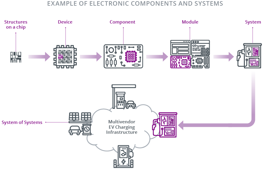
Designing such artefacts requires an interdisciplinary hierarchical approach, whereby various ECS specialists are working at different abstraction levels. As a result, the same term can have different meanings for specialists of different ECS domains: for instance, a “system” designed and implemented within a given development process may be integrated as a “component” into a higher-level “system” within another development step of the engineering process. Nevertheless, to avoid confusion, since 2021 the ECS-SRIA includes a glossary, where many of the key terms are defined, to avoid inconsistency across the various chapters. It was also felt that developing a common language was important in building a strong and integrated ECS community. In addition, some of the bricks of the ECS technology “stack” are further detailed below.
- Device: in the context of the ECS-SRIA, and if it is not further qualified, a device will be defined as a “packaged chip”, whether it is a packaged integrated circuit (e.g. system on a chip, memory, processor, or microcontroller) or a micro-electromechanical system (MEMS)/micro-opto-electro-mechanical system (MOEMS). A device performs a general electrical, electronic or electrical/electronic/physical transduction role.
- Component: a combination of devices and other elements (such as passives) that fulfil a specific need, such as transduction of a single physical parameter within a well-specified case. A component is not self-contained in all its functions, as it requires the close support of other components for operation (e.g. in data processing, power handling, and embedded software).
- Module: a combination of correctly integrated components in which their assembly embodies a specific functionality required for the proper working of a system (e.g. sensing and actuation module, control module, communication module, energy provision module). A module is self-contained in hardware and software, making it interchangeable between systems, and allowing a higher abstraction level in systems design.
- System: for the purpose of this SRIA, a system is a set of electronic-based constituents (subsystems, modules and components, realised in hardware, software, or both) that are integrated in a way that allows the system to perform a desired (set of) function(s). Due to ECS typically being constructed hierarchically, a “module” (e.g. camera or other sensor) being part of the electronic “system” in an autonomous car might itself be referred to as a “system” when being designed (e.g. while integrating lower-level components together to achieve the “camera” function).
- System of Systems (SoS): a collection of independent and distributed embedded and cyber-physical systems dynamically composed to generate a new and more complex system, provided with new functionalities and driven by new goals not present in the constituent embedded and cyber-physical systems individually. The difference between a “system” (comprising subsystems, modules and components) and a “System of Systems” (also comprising subsystems) is that the subsystems of a system are chosen and integrated during design-time (i.e. completely under the control of the engineers), while in a System of Systems the constituent (sub)systems are physically independent and dynamically form a System of Systems at run-time.
The structure
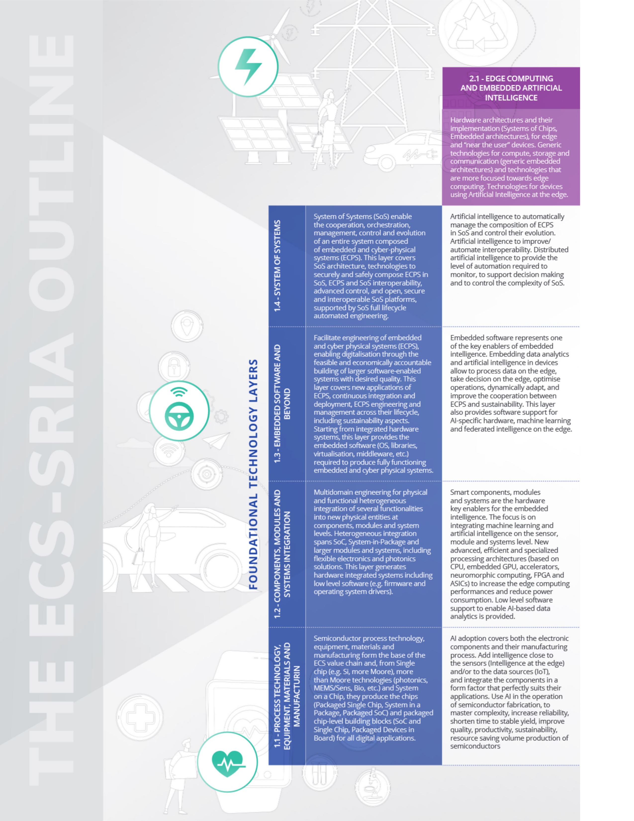
The first part of the ECS-SRIA is composed of four chapters focused on the Foundational Technology Layers and their technical challenges along the technology stack, from materials and process technology to components, modules and their integration into electronic systems, embedded software developments and software technologies, to full systems and Systems of Systems. These foundational layers are characterised by hierarchical dependencies due to the inherent nature of ECS and the way they compose and integrate in complex structures. Advances in all Foundational Technology Layers will be essential to creating new electronic chips, components, modules, systems, and systems of systems along the value chain: these are the fundamental elements required to build the digitalisation solutions of the future.
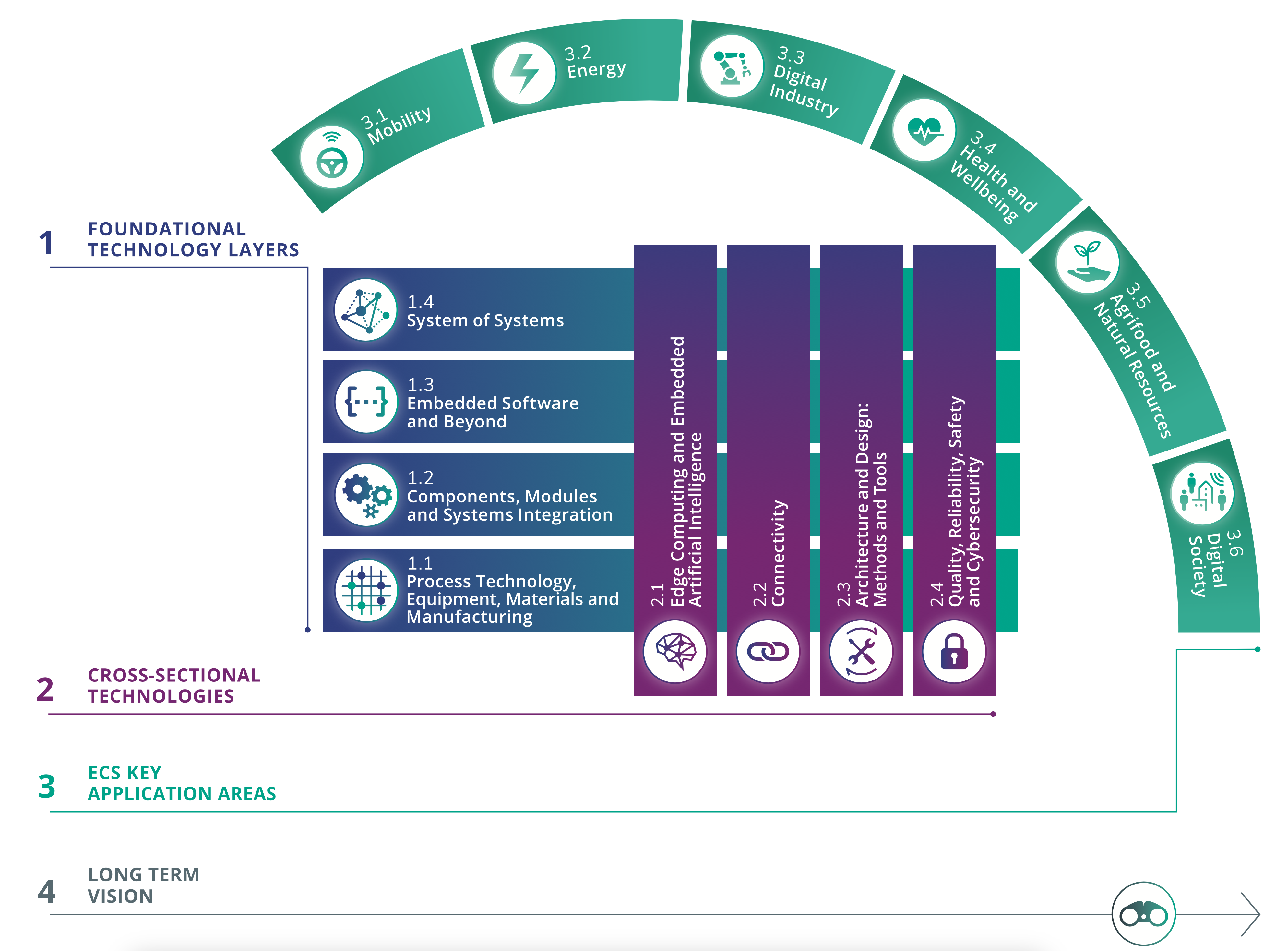
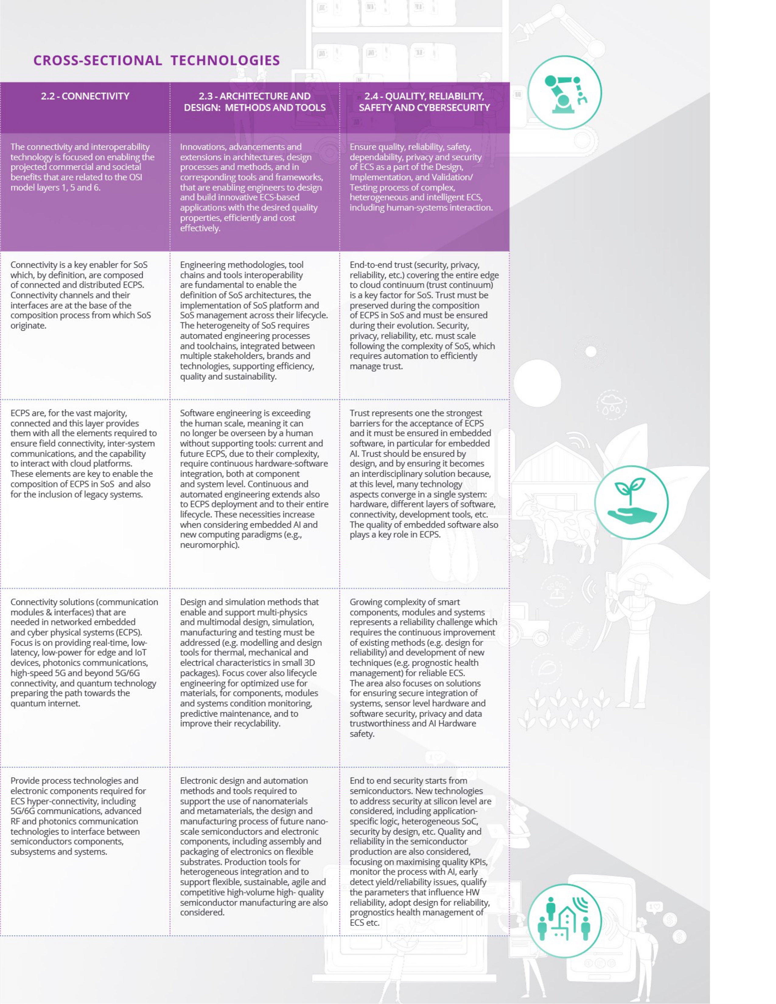
The foundational layers represent a very fertile ground where new interdisciplinary technologies, products and solutions can grow. They are then complemented in the second part of the ECS-SRIA by four Cross-Sectional Technology chapters that focus on transversal areas of scientific research and engineering, where innovative results emerge from the joint contribution of the foundational layers to those specific areas. Edge Computing and Embedded Artificial Intelligence, or Connectivity (e.g. 5G to 6G) will require new integrated circuits to develop innovative electronic components that can be used to develop smarter and more connected components, modules and entire systems, running smart software that will offer new functionalities and capabilities. That will allow these systems to interact, cooperate and merge in larger systems of systems. Similarly, Architectures and Design: Methods and Tools have to be further developed to provide support to each of the foundational layers, covering all domains along the technology stack, across the entire lifecycle of technologies and products. The same applies to Quality, Reliability, Safety and Cybersecurity concepts that can only be addressed successfully if they are encompassing the whole ECS process flow along the entire value chain.
The innovation generated by these cross-sectional technologies will be applied across foundational layer stacks and amplify the effect of innovation in all key ECS application domains. Of course, there is some overlap among the eight technology chapters since they are closely linked, but as they examine the individual challenges from different perspectives, this overlap is extremely constructive and generates valuable synergies.
In the third part of the ECS-SRIA, six Application chapters describe the challenges arising from specific ECS application domains that are key for Europe and identify the R&D&I efforts required by these application domains as regards ECS.
Finally, the Long-Term Vision chapter illustrates our vision of the ECS beyond the time horizon covered by the other chapters. It seeks to identify the research subjects that must be addressed at low TRL levels as foundation and preparation for the crucial developments in European industry over the next decade. Based on the trends and plans described in the preceding chapters, the long-term industrial requirements are also examined to help research programmes understand which hardware, software and system solutions should be produced most effectively for the continuous improvement of European digital technology.
As mentioned, the ECS covered by this document is very wide-ranging, and involves many technical disciplines in materials, processes, hardware and software. This means not many will understand all the technical details presented in the ECS-SRIA, and most readers will only want to read those chapters that cover the disciplines of their interest.
The structure of all the Foundational Technology and Cross-Sectional chapters is identical. This forms the basis for the authors to explore each application area from a different perspective, with the intention here being that the application demands are the main focus, not the technical challenges.
A Glossary describing the terms used in the document, as well as a List of Acronyms used in the document, can be found in the Appendix. The Analytical Index available in the previous releases of the ECS-SRIA has been substituted by an advanced Search functionality. At the end, the reader can also find a List of Contributors who collectively wrote this ECS-SRIA.
Finally, to highlight the synergies/links between the chapters and provide hints to the reader, cross-references have been introduced alongside the text.
Cross-references consist of the chapter icon and appear alongside the text. When hovered on, they indicate the relevant chapter number and the topic or concept described in the text is also highlighted. When clicked on, they will navigate you to the referenced chapter.
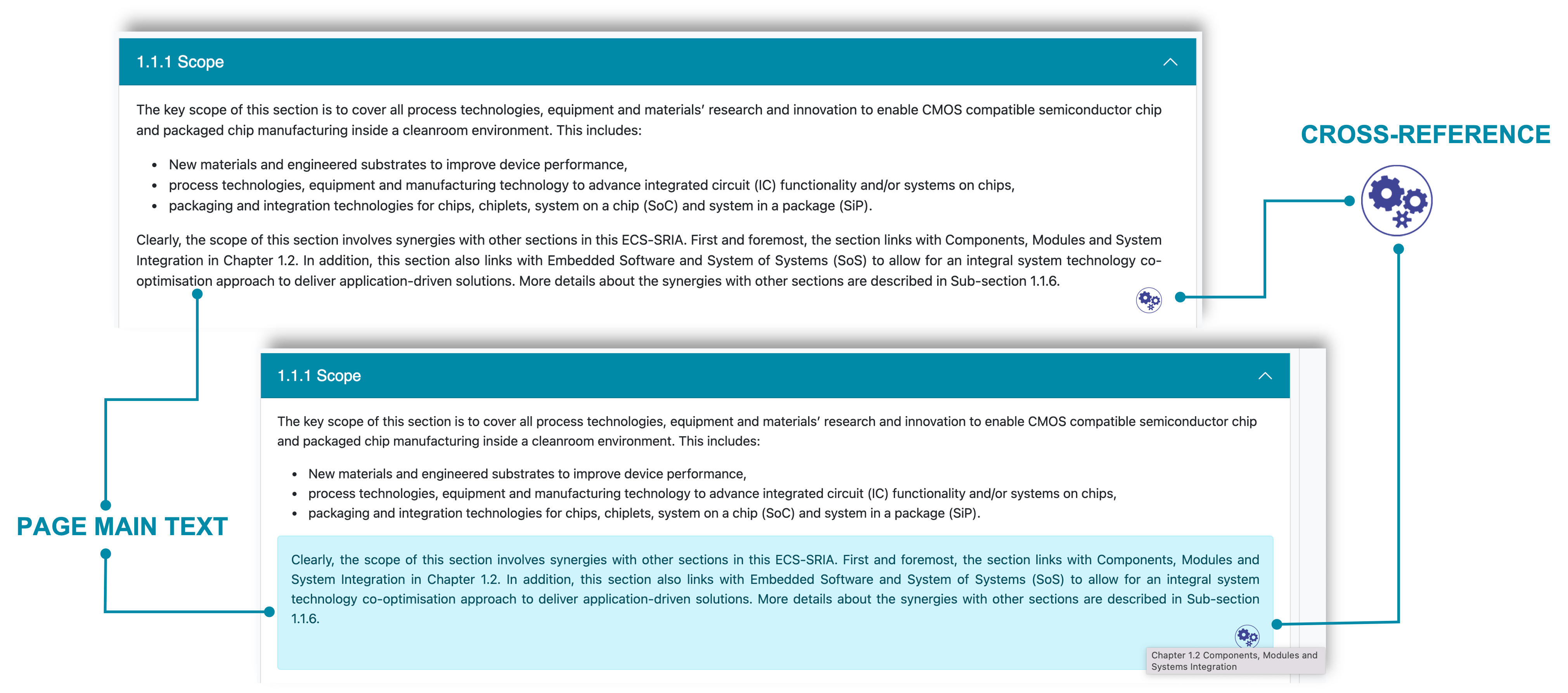
References within a text are indicated by small numerical markers embedded in the content, e.g. 0. Upon clicking one of these markers, readers are instantly directed to the corresponding entry within the References section. This feature allows readers to seamlessly access the sources from which the information has been derived.
Furthermore, by clicking on the same footnote number located in the References section, readers can effortlessly return to the exact point within the main text where the reference was initially cited. This interactive function not only enhances the reader's comprehension but also streamlines the process of verifying and exploring the sources behind the presented information.
In this ECS-SRIA, the Major Challenges identified by the different chapter teams were analysed and merged into four Main Common Objectives for the ECS community. In addition, three common Roadmaps covering the short term (up to 2028), medium term (from 2029 to 2033) and the long term (2034 and beyond) provide the key milestones derived by the chapter teams.
Main Common Objectives
For each technology and application domain, the ECS-SRIA identifies specific challenges, with a focus on the most critical aspects to be tackled from the perspective of innovation. The analysis of each challenge illustrates the state of the art of the associated technology and/or application domains, describes the vision of the ECS community for the future, identifies potential outcomes, and defines research and engineering activities on the key focus areas that are fundamental to successfully address the challenge.
Across this document, 68 different Major Challenges are identified that have emerged from the analysis of the foundational technologies, the cross-sectional technologies and the key application areas. The Major Challenges are frequently interdependent – they influence each other, become increasingly demanding, and have an impact on many areas, including technology innovation, industrial competitiveness, security, safety, business and environmental sustainability, society, etc. From this perspective, the Major Challenges represent key factors for the achievement of the four Main Common Objectives, which are aligned with the European Commission’s strategic priorities (see table in Appendix).
Main Common Objective 1: boost industrial competitiveness through interdisciplinary technology innovations
Electronic components and systems, by their inherent nature, are the result of interdisciplinary research and engineering. These require competencies in diverse technology domains, including process technology, equipment, materials and manufacturing, electronics, and telecommunications, as well as cross-sectional technologies such as edge computing, artificial intelligence, high-speed connectivity, and cybersecurity. One major strategic trend is the evolution to the use of Open-Source Hardware and Software, whereas RISC-V based architecture solutions will become an asset of a competitive nature for the European industry.
ECS technologies are turning each digital component and equipment into an intelligent cyber-physical system, thereby driving new market demand. Embedded platforms for automotive (electric mobility, autonomous driving, etc.), industrial (Industry 4.0, IoT for agriculture, etc.), medical (medtech for connected patients, etc.), and energy (new energy-aware ECS and more flexible energy management, etc.) will rely extensively and increasingly on ECS technologies.
These trends compel ECS research to be interdisciplinary to benefit from the multiple available sources of innovation, as well as to be research-intensive and market-oriented. This will ensure forthcoming ECS innovations will be of strategic value for Europe and boost its industrial competitiveness in all its value chains, and help building the strong industrial base essential for European strategic autonomy.
With the Chips Act, the KDT JU transits to the Chips JU, with a mandate extended to capacity building activities and related research and innovation activities of four operational objectives of the Chips for Europe Initiative, as set out in the Chips Act article 4:
-
building up advanced design capacities for integrated semiconductor technologies;
-
enhancing existing and developing new advanced pilot lines across the Union to enable development and deployment of cutting-edge semiconductor technologies and next-generation semiconductor technologies;
-
building advanced technology and engineering capacities for accelerating the innovative development of cutting-edge quantum chips and associated semiconductor technologies;
-
establishing a network of competence centres across the Union by enhancing existing or creating new facilities.
These objectives translate in particular into the following additional activities for the JU:
-
The development of new capabilities to design, prototype and test innovative chips through pilot lines on semiconductor technologies, with the close collaboration of European RTOs and industrial vertical sectors.
-
The establishment of competence centres, which will address the lack of skills that is affecting the European labour market, trying to provide training support for future professionals in the whole ECS domain, consolidating and strengthening the rich knowledge base required by interdisciplinarity.
-
The setting up of a new Virtual Design Platform and specific funding instruments which will provide support to the rich, diverse and multidisciplinary ecosystem of European SMEs and start-ups, facilitating investments in research, development, and production and simplifying the process of bringing innovation from “the lab to the fab”.
This SRIA is the reference document for all research and innovation activities of both the former (under KDT) and these new Chips JU activities. This extension reflects the intrinsic interdisciplinarity of the SRIA and further strengthens it from different perspectives.
All the new initiatives introduced by the Chips Act have been conceived to boost European competitivity in the ECS market and ECS-based application domains, guiding investments and resources towards strategic areas of semiconductor technology that are most critical for the European industry's competitiveness. This SRIA contributes to the identification of these critical areas and of the associated challenges that will characterise their development in the next ten years. The role of the SRIA is fundamental to identify the key starting points for R&D&I and to setup multi-annual synergies with the pilot lines that will focus on more mature prototyping. The SRIA will also potentially provide the elements for the “first-of-a-kind facilities” envisioned by Pillar 2: the synergies between these three steps represent the key strategy to increase European capacity building, to boost competitiveness, and to anticipate, prevent and effectively manage future crises.
Main Common Objective 2: ensure EU digital autonomy through secure, safe and reliable ECS supporting key European application domains
A strong, competitive and sovereign ECS industrial and technological base will help Europe to:
- Fulfil its own digital technology needs in a way that reflects its interests and values.
- Improve the resilience of its critical infrastructure and ICT systems.
- Develop its ability to shape international rules, norms and standards.
European strategic autonomy will rely on a trustworthy and virtuous cycle by supporting the development of innovative ECS technologies focused on security, safety, reliability, dependability and privacy.
These innovative technologies will simplify the implementation of the European Strategy for Data3, 4, and ensure security, privacy-by-design and strategic autonomy all along the industrial and digital value chains. Such technological innovation will also enable the design and development of secure, safe, reliable, dependable, privacy-compliant electronic components and systems, as well as generate new requirements that will drive the development of new technologies, restarting the cycle.
Threats to Europe’s strategic autonomy are to be found in the microelectronics value chain, and downstream in the component user segments of the electronics industry. In this context, the Major Challenges identified by the ECS-SRIA will help develop innovations in secure, safe and reliable ECS technologies for creating EU-based/ made solutions in the key European applications domains of:
- Aerospace, defence, security.
- Automotive, transportation.
- Machinery, robotics, electrical equipment, energy.
- Communications, computing.
- Healthcare and well-being, etc.
European technology-based, secure, safe and reliable ECS, combined with European AI solutions, are critical to securing global leadership and strategic autonomy in key areas such as ICT and to ensure compatibility with EU values.
The Chips Act aims at consolidating and strengthening European strategic autonomy, extending and boosting the KDT with a new specific focus on the upstream of the ECS value chain. Reducing the dependency on non-European suppliers and avoiding future shortages represent the main steps towards strategic autonomy: reaching the independence on non-European suppliers for critical ECS is crucial for ensuring that European industries and key application domains have a stable supply of semiconductors, even during future global disruptions or geopolitical tensions. Technological leadership and strategic autonomy are the primary ingredients required to:
- Control ECS manufacturing to produce solutions designed to meet stringent security requirements; an essential aspect for maintaining secure digital infrastructures and key applications (e.g. automotive, defence, energy, etc.).
- Ensure resilient supply of semiconductors produced in Europe to support the resilience of critical infrastructure, including energy, transportation, and healthcare systems, which rely on advanced chips.
- Achieve a greater control over the technology infrastructure that underpins the European digital economy, ensuring that critical data and systems remain under European jurisdiction.
- Enhance Europe's economic competitiveness, leading to the creation of high-tech jobs, stimulating innovation, fostering economic growth, and making Europe less dependent on external economic forces.
Main Common Objective 3: establish and strengthen sustainable and resilient ECS value chains supporting the Green Deal
European strategic autonomy will also require the sustainability and resilience of the entire ECS value chain since the development of innovative technologies focused on sustainability and the Green Deal will support ambitions to achieve a green, resilient and competitive Europe.
Moreover, the serious effects of climate change that we are experiencing daily and the current geo-political situation, which highlights our dependency on non-European fossil energy providers, further reinforce the need for Europe to accelerate its transition to climate neutrality by 2050.
This challenge must be perceived as an opportunity to create a new environment for boosting innovative aspects of technology and business models through achieving the following:
-
Relying extensively on ECS-based technologies and digitalisation as key factors for lowering our global energy footprint at all levels of the economy, and by placing sustainability at the heart of combined digital and green transitions.
-
Positioning the European players in hardware as front-runners in sustainability to secure a wider market so they can become world leaders. This will need European companies to consider the circular economy, new market positioning (by turning small market shares into specialisation areas), the environmental impact of global manufacturing, etc.
-
Establishing this carbon-neutrality challenge, based on a close link between the digital and green transitions at the core of future funded collaborative research and innovation in ECS. This will help ensure a positive impact for each stage of the value chain, and to achieve carbon neutrality right down to the final application/digital service.
This new context is required to fight and reduce the effects of climate change.
Pillar 1 of the Chips Act will contribute to the development of new materials, new manufacturing processes, advanced devices and a higher level of integration, which impact significantly on the power consumption of ECS, on the sustainability of their design and manufacturing, and on ECS-based applications, contributing the objectives of the Green Deal. Sustainability and green are considered as a transversal objective addressed by all the technology and application domains covered by this SRIA, which has already identified the challenges that must be tackled by the new technologies that will be developed within Pillar 1 in the next years (e.g. FDSOI, heterogeneous integration, new design methods and tools, etc.). But the benefits of the Chips Act will extend beyond the pure technological aspects:
-
Promoting the principles of a circular economy in semiconductor manufacturing can be a significant step. This might involve designing chips for longevity, enabling easier recycling, and minimizing electronic waste.
-
Encouraging the use of sustainable materials in chip production can reduce the environmental impact. This could involve sourcing low-impact materials, using recyclable substrates, and adopting eco-friendly packaging. This extends also to promoting environmentally friendly manufacturing practices, which can reduce the environmental footprint of chip production (e.g. renewable energy sources, reduction of water and resource use, etc.), reduction of CO2 and other greenhouse gas emissions, better recycling and more responsible disposal practices for electronic components and waste.
-
The strategic autonomy introduced by the Chips Act contributes to economic sustainability and security, through a reduced dependency on non-European suppliers, an increased production capacity, more competitive manufacturing processes and products, a resilient supply chain, circular economy promotion, etc.
-
A sustainable semiconductor industry is also vital for supporting the sustainability goals of the application domains based on ECS, such as those related to renewable energy, electric vehicles, digital industry and sustainable agriculture.
Main Common Objective 4: unleash the full potential of intelligent and autonomous ECS-based systems for the European digital era
ECS must have intelligence and autonomy capabilities to control their complexity more efficiently and more cost-effectively. This will help provide novel advanced functionalities and services, limit human presence to only where it is strictly required, improve the efficiency of vertical applications, etc. Intelligence and autonomy are also required for the role of ECS in the application domains, representing an important factor for the sustainability and resilience of the value chains: an ECS-based system that provides intelligent energy management, relying on technologies such as AI, represents a key building block – for example, for smart home and energy applications. Moreover, it also improves the resilience required to ensure optimal energy consumption in critical conditions and contributes to the sustainability of the value chain associated with vertical applications, since it reduces operational costs, environmental impact, improves the quality of service (QoS), return on investment (ROI), etc., thereby strengthening the global competitiveness of European companies and helping to achieve the objectives of the EU’s Green Deal.
The Chips Act will allocate significant resources for R&D&I, supporting the development of cutting-edge semiconductor technology that will be crucial to unleash the power of AI: for example, higher levels of integration will contribute to the diffusion of AI, specifically on the edge where the right ratio between dimensions, energy consumption, computing power and cost makes the difference. With an innovative and strong semiconductor industry Europe could improve its competitiveness in the global AI landscape, and this could contribute attracting AI talent, companies, and research initiative in Europe. The Chips Act resources will also be crucial to consolidate the European future position in the AI market and contribute to the supply chain resilience, supported by a robust semiconductor industry in AI hardware. The new resources will boost the R&D&I activities described in Chapter 2.1 of this SRIA, potentially accelerating the related timeline, and ensuring a solid support for all the vertical domains covered by the Application chapters.
Ensure engineering support across the entire lifecycle of complex ECS-based systems
Modern ECS-based systems are complex, and they cannot be properly elaborated and used without the appropriate engineering support across the entire lifecycle, from requirements analysis to design, development, deployment/commissioning, operation/management, remote-maintenance repair and overhaul, retirement/recycling and evolution.
Engineering support represents a key factor for achieving the four Main Objectives as it:
-
Impacts industrial competitiveness by simplifying life cycle management, and improves the quality of the engineering process, making it more cost-effective and agile.
-
Simplifies and improves the development of trustworthy ECS technologies, products and applications.
-
Supports sustainability and resilience that reduce lifecycle management costs, as well as ensuring the automation and continuity of operations.
-
Is fundamental to unleashing the full potential of intelligent and autonomous ECS, which requires completely new approaches to engineering, design and development methodologies, as well as toolchains and tools.
-
Improves professional training and education by strengthening and developing new and specific skills.
ECS engineering plays a key role in Pillar 1 of the Chips Act, which includes specific instruments to support the engineering process, specifically in the critical area of new chips design, to increase design activities and create a strong design ecosystem in Europe. A Virtual Design Platform (VDP), providing design tools, an IP library for various technologies, and PDKs to access the fabs, will be established to simplify and accelerate the process of going “from the lab to the fab”, and make that process more accessible for EU companies, start-ups and SMEs, especially fabless. Specific Design Enablement Teams (DET) will support this process providing targeted assistance on designing chips and more complex systems, with the presence of experts in the design flow, foundries, and pilot lines, from virtual prototyping via tape-out and engineering samples to high volume production. To this regard, Competence Centres will be established to address the skills challenges that Europe is experiencing and provide education and professional training solutions for the next generation of chip designers: DET and a Competence Centre will provide advice, training, and skills-building solutions, supported by the industry-grade training framework offered by the Virtual Design Platform. Chapter 2.3 and other chapters address many of the R&D&I challenges that the VDP and Competence Centres will have to face in the next decade.
Artificial intelligence topics in the ECS-SRIA
While not a totally new topic (it is used for example in several embedded system for vision, enabling autonomous vehicles), Artificial Intelligence really came to the forefront for the public at large in 2023, with tools such as Chat-GPT (released for public use only on November 30th, 2022) and other generative AI (Dall-E, Stable Diffusion) that grabbed the headlines in mainstream media. The ECS Research and Innovation roadmap interacts with the development of AI tools and algorithms in two symmetrical ways: ECS are an enabler for new AI developments, and AI can in turn be a significant enabler for new ECS advances. Those two aspects are extensively discussed in this current edition of the SRIA.
-
ECS as enabler of AI: Chapters 1.1 and 2.1, as well as the Long Term Vision Chapter, stress the importance of moving the processing of AI algorithms locally on a hardware device (in deep-edge devices, edge devices or on-premises computing resource depending on the application) close to where the data is generated (e.g. by a sensor), a trend known as “embedded AI” or “edge AI”. Benefits include reducing the energy consumption of the data infrastructure by transmitting only relevant data or pre-treated information, improving data protection, increasing security and resilience due to a reduced reliance on telecommunication links, reducing latency, and decreasing memory footprint. Many of the focus research areas identified in Major Challenge 1 (Advanced computing, memory and in-memory computing concepts) of Chapter 1.1 support this move towards AI at the edge. More generally, energy consumption of AI solutions is a significant issue due to the expected widespread increase of their usage, and new concepts and architectures (bio-inspired and other ones) must be explored to respond to it. Likewise, the four Major Challenges (increasing energy efficiency, managing system complexity, increasing device lifespan and ensuring European sustainability in AI) identified by Chapter 2.1 all cover research topics which will enable the development of a strong European embedded AI ecosystem.
-
AI as enabler of ECS: this aspect is discussed in Chapter 2.3, where several examples of AI use are listed to tackle Major Challenge 3 (managing complexity), such as AI-based methods for the architecture exploration and optimisation, to achieve a global optimum, AI-based guidance in the V&V process, and automatic generation of test cases with AI support. Moreover, in its entirely new section devoted to Machine Learning and Artificial Intelligence, the Long Term Vision Chapter states that AI/ML methods are increasingly adopted in design space exploration at several stages of circuit design, as well as in design testing and verification. The potential of these AI-based methods is not limited to circuit design and extend to large scale ECS products encompassing HW and SW, as well as multi-physical, distributed systems. They are also expected to provide guidance to engineers in multi-risk (safety, security, privacy, and other trustworthiness risks) optimisation problems. Gathering / generating the appropriate data to train the models is identified as one of the most difficult issues to be addressed.
A third aspect is that AI adds complexity to the systems it empowers. This in turn raises additional issues at the design phase, as addressed by Chapter 2.3. There, Major Challenge 1 (Extending development processes and frameworks to handle connected, intelligent, autonomous, evolvable systems) and Major Challenge 2 (Managing new functionality in safe, secure and trustworthy systems) stress the need to develop new design and verification and validation methods for AI-based ECS, including ECS evolving during lifetime.
Finally, a purely technical approach to develop trustworthy and explainable AI, or having AI in the loop with verification of its results might not be enough to address the growing public concerns about the potential dangers of AI (pushing many governments across the world to sign the Bletchley Declaration on AI safety). In the years to come, cooperation between multidisciplinary partners with backgrounds in AI, ECS and social sciences, as well as access to “foundation models” by European academia and industry will be required to achieve and ensure the acceptance of efficient and responsible AI-based ECS, reflecting European values.
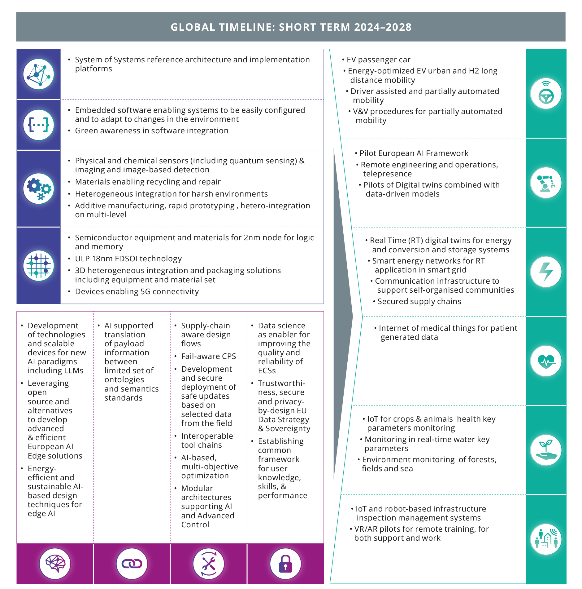
The ECS-SRIA 2024 lists a number of milestones to be reached in the short term (2024–2028), medium term (2029–2033) and long term (2034 and beyond) via collaborative research projects across Europe, reflecting the ambition of the ECS industry towards the achievement of the four Main Objectives identified above.
The following figures summarise the most salient milestones to be reached in the various domains covered by the ECS-SRIA over the three time periods:
-
Short term (2024–2028)
The industry has a precise idea of what will be achieved during this short-term timeframe.
-
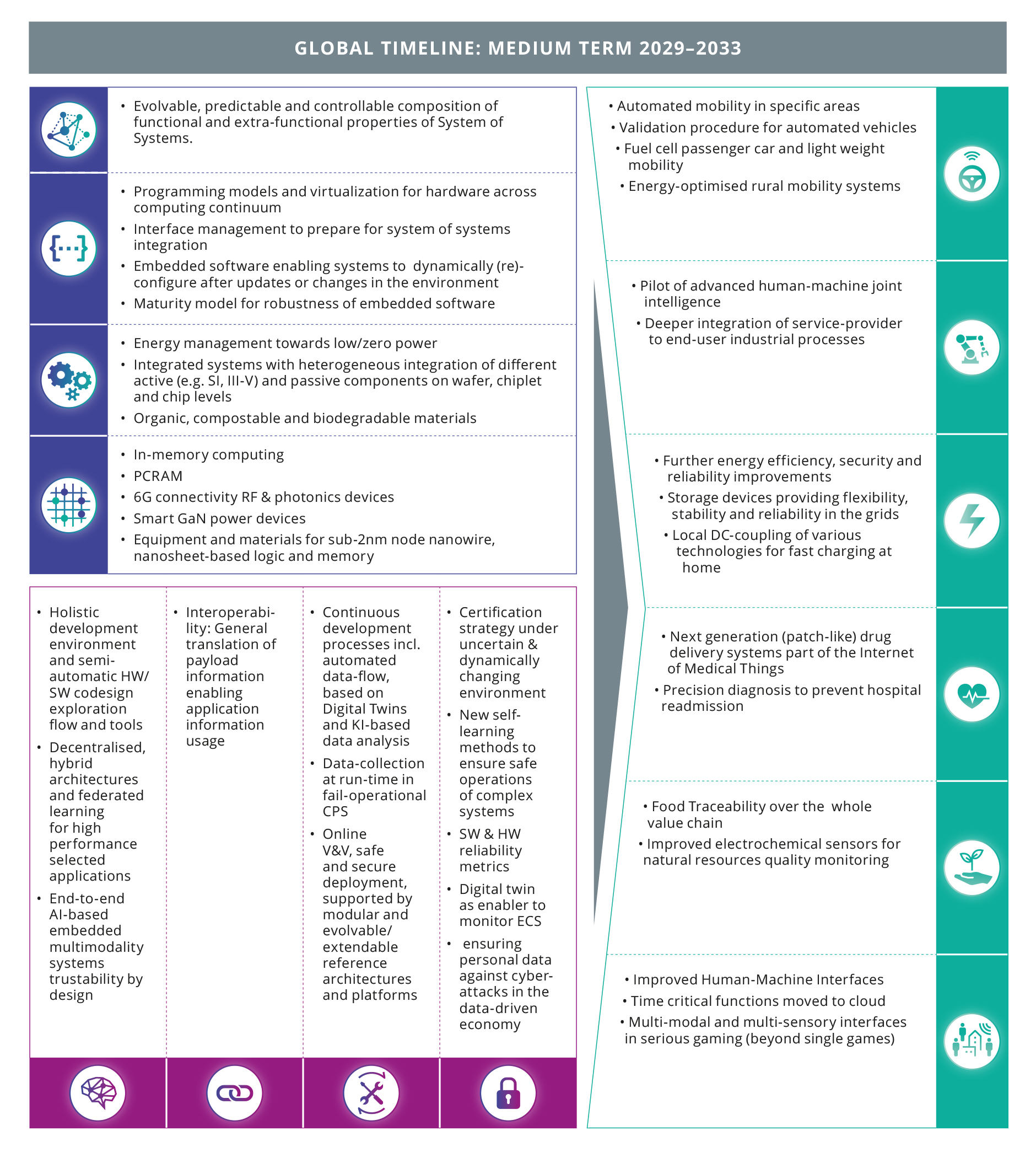
Medium term (2029–2033)
There is still reasonably good knowledge of what can possibly be achieved. -
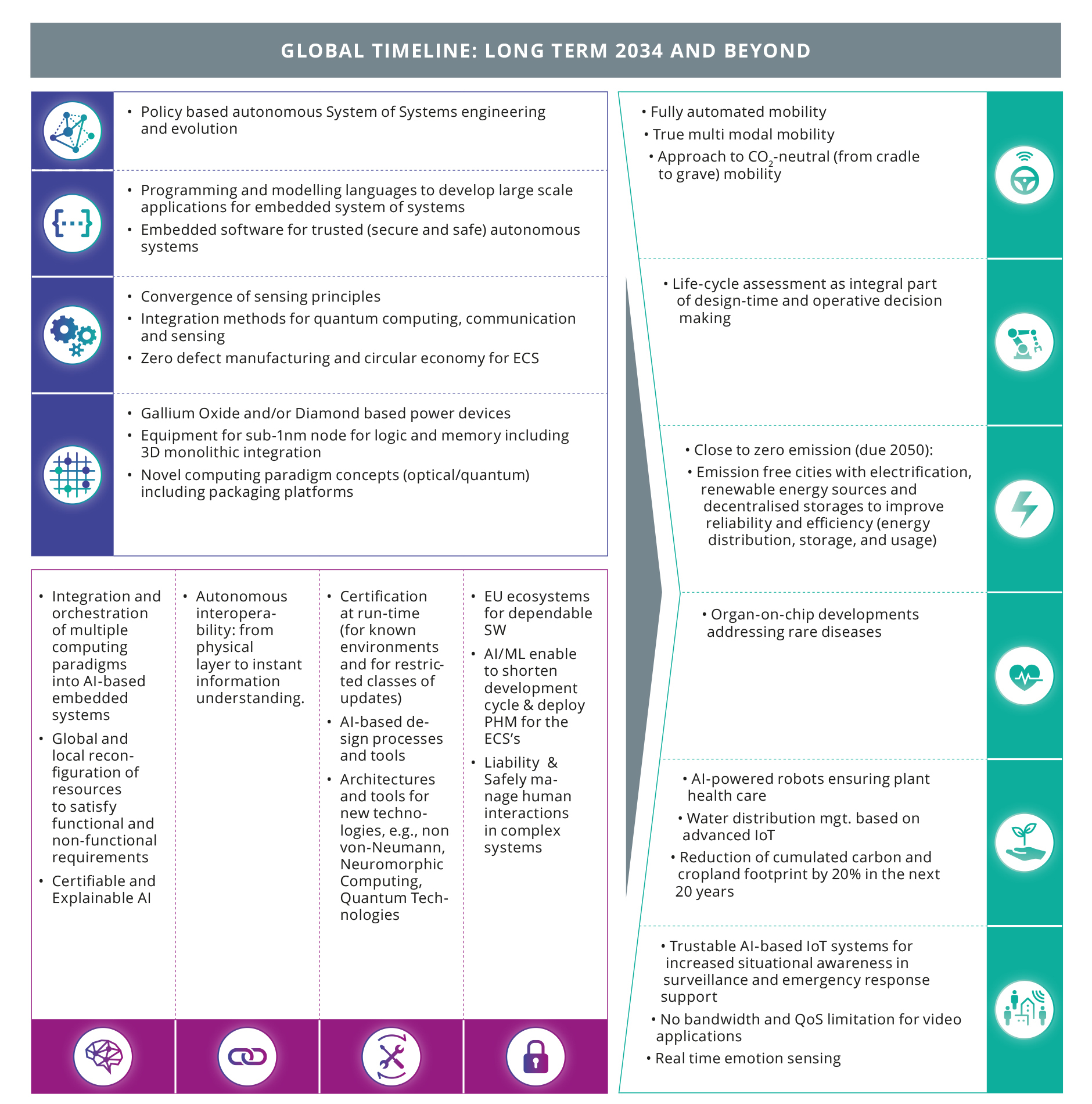
Long term (2034 and beyond)
Expected achievements are more of a prospective nature.
Including a milestone in each of these time periods means that the described features are expected to be available at TRL levels 8–9 (prototype or early commercialisation) within that timeframe. For example, the Components, Modules and Systems Integration Chapter expects that, within the next five years (short term). The materials that enable recycling and repair will be available. These materials will allow for the deployment of the monitoring of forests, fields and oceans, as envisioned by the Agrifood and Natural Resources Chapter over the same time horizon. In parallel, this monitoring will gain in efficiency due to the development of advanced AI edge solutions leveraging open source or alternative strategies, as forecast by the Chapter on Edge Computing and Embedded Artificial Intelligence.
The above example also clearly shows that progresses in the various domains covered by the ECS-SRIA are deeply interconnected. Innovation in one area is building upon, or being driven by, innovation in other areas. Similar examples could, of course, be developed for the other time horizons, as represented in the Figure 0.4, Figure 0.5, Figure 0.6.
More detailed diagrams, including additional milestones, are presented in the individual chapters.
Electronics components and systems are key digital technologies enabling the development of numerous applications. As such, the ECS research and innovation priorities are significantly driven by application roadmaps and needs. To that effect, the Key Application Areas part of the ECS-SRIA translates application roadmaps into requirements for ECS. Conversely, the Foundational Technology Layers part maps out future advances and potential new breakthroughs in applications. The ECS-SRIA therefore promotes synergies with many neighbouring application-oriented communities. For example, the Mobility Chapter ( 3.1) has strong links with ERTRAC; the Digital Industry Chapter (3.3) with EFFRA; and the Agrifood and Natural Resources Chapter (3.5) with the working group of the Alliance for the Internet of Things Innovation (AIOTI) in Smart Farming and Food Security, and with Water Europe4. In each case, experts participated in the work of both groups. There are also close interactions and alignments with European PPP initiatives, such as 2Zero and CCAM, IHI, etc.
The Cross-Sectional Technologies part also leverages the links of the ECS community with other technology-oriented domains, such as the European Technology Platform for High Performance Computing (ETP4HPC), EuroHPC, the European Working Group on High-Performance RISC-V based reference processing architectures, and Big Data Value Association (BDVA), with strong relations with the Edge Computing and Embedded Artificial Intelligence Chapter (2.1). Likewise, the Connectivity Chapter (2.2) benefited from fruitful exchanges with the 5G Infrastructure Association, SNS and inputs from the European Cyber Security Organisation (ECSO), as reflected in Chapter 2.4.
Several contributors of the Technology parts are also actively involved in the elaboration of international roadmaps (e.g. the Heterogeneous Integration Roadmap (HIR)5 in electronic packaging and integration, the IEEE International Roadmap for Devices and Systems (IRDS)6 for the semiconductor industry), and the RISC-V Roadmap of RISC-V International7 and the European Working Group8.
To summarise, this ECS-SRIA combines application-pull and technology-push with the objective of enhancing the fertile dialogue between technologists and technology users, and strives to include discussions of upcoming strategic value chains.
The following diagram provides an outline of the entire ECS-SRIA to clarify the roles of the chapters, the technology domains they cover and the synergies between them, simplifying the comprehension of the ECS-SRIA and its “navigation”.
By themselves research projects contribute partially to resolve societal challenges and to create economic value for Europe. The full leverage of several research projects with significant impact for EU regarding societal and economic impact will happen only if several “innovation accelerators” are in place, which will bring the research results to market. Standardisation and regulation, education and training, international cooperation, and research infrastructures are a few of these accelerators.
Discussing those topics is beyond the scope of the ECS SRIA, which is the expression by the industry of its Research and Innovation vision. In essence, the SRIA is designed to be funding instrument agnostic, so that it can constitute the basis of calls for various programmes, such as Horizon Europe, Eureka, or national initiatives. That being said, some of the accelerators listed above are being set up in the frame of the Chips Act, and we cannot ignore that context. We refer here specifically to the Design Platform and the Pilot Lines included in the Chips for Europe Initiative, which has the objective of supporting and accelerating technological capacity building and innovation in the Union by bridging the gap between the Union’s advanced research and innovation capabilities and their industrial exploitation.
The pilot lines are intended to allow companies and academic institutions to perform research on future technologies. By having prototyping capabilities, they allow to assess the feasibility, performance, and reliability of their novel electronic devices, components and modules, or of new manufacturing processes, without affecting ongoing production – in case of industrial pilot lines, or enabling research institutes to showcase their innovations and speed up the time-to-acceptance into the market. SME support via low-volume prototyping is another potential benefit of pilot lines.
Moreover, as pilot lines often involve collaborations between industry partners, research institutions, and academia, they will be fostering the exchange of knowledge, expertise, and best practices in electronics manufacturing to tie these stakeholders more closely together. In this context, pilot lines will also contribute to workforce training, as they will offer hands-on experience and exposure to state-of-the-art technologies and practices. Those collaborations will also pave the way for fast transfer to volume manufacturing ensuring European competitiveness and growth in EU-based share in microelectronics.
While it is outside of the SRIA scope to indicate how these research infrastructures and services should be run, it is important to ensure that their implementation most effectively supports the research needs exposed in the SRIA. To that effect, the following table identifies, for the Design Platform and for the Pilot Lines most likely to be launched in a first batch (as of the time of writing of this addendum to the 2023 ECS SRIA edition), research topics which are expected to be supported by those instruments. Note that the pilot line mechanism is meant to support a large variety of developments, from device manufacturing in semiconductor processes, MEMS, packaging and hybrid integration (SiP), as well as module and system level development. It is therefore expected that other pilot lines, beyond the ones considered here, and focusing on different technologies and different steps in the value chain, could be implemented in later phases.
| Design platform | Advanced 2nm and beyond | FD-SOI | Advanced Packaging and Heterogeneous Integration | Other pilot lines | |
|---|---|---|---|---|---|
| 1.1 Process Technology, Equipment, Materials and Manufacturing | Launching ground for new processes, equipment technologies and materials | Low-power consumption, radiation hardness, More than Moore app. | Introduce materials and process innovations as well as advanced manufacturing, test and inspection equipment for future AP/HI systems. | ||
| 1.2 Components, Modules and Systems Integration | Improve design capabilites to become a closed loop (i.e., to include feedbacks from the production process and from the field use, respectively) as well as define the new sets of interfaces for the complex integration solutions at die / module / system levels as needed for implementing heterogeneous and chiplet approaches - in particular for ECS applications that will be exposed to demanding and harsh environments (as these ECS are essential for our European backbone industry -automotive, energy, industry, health, ...- and not sufficiently and securely addressed by the worldwide leading players). | Impact of advanced node inflections like backside power distribution networks, forksheet, CFET and 2D material channels 3D heterogeneous integration in chiplet implementation |
Enable enhanced and diversified functionalities (e.g. combined sensing, processing, communication, ...) in small form factor electronic components and systems. | Platforms leading to the scalability of elements enabling connection between the digital and physical worlds (e.g. MEMS, integrated photonics, power electronics, quantum approaches…) in silicon or silicon alternative technologies will provide, together with logical circuitry, additional essential building blocks to be integrated in full fledged electronic systems | |
| 1.3 Embedded software and Beyond | Design Technology Co-Optimisation | Design Technology Co-Optimisation | |||
| 1.4 System of Systems | System Technology Co-Optimisation | System Technology Co-Optimisation | |||
| 2.1 Edge Computing and Embedded Artificial Intelligence | Provide non-differentiating IPs (I/Os, memory interfaces, etc) Support the Open Source Hardware community in Europe Provide tools for embedded AI, such as tools allowing to quantize and decrease the size of Neural Networks for embedded accelerators |
Drive PPACE (Power - Performance - Area - Cost - Efficiency) improvements for advanced nodes to increase the energy efficiency of computing systems Research PDK’s to support managing the increasing complexity of systems |
Energy efficiency, embedded non-volatile memories | Advanced packaging technologies allow the integration of diverse and specialized components such as processors, GPU/FPGA, memory, sensors and communication chips in a single package. This enables new, more powerful and energy-efficient edge computing, AI and communication solutions in small form factors. | |
| 2.2 Connectivity | * Enable the development of power efficient connectivity solution leveraging European-based semiconductor technology * Enable the development of innovative connectivity solution at mmW and THz frequencies |
* Enable a European ecosystem that can support heterogeneous integration (multi-die system in a package, advanced assembly capability, advanced substrate manufacturing, etc.) to help European players capture higher value in the connectivity market. * Enable the development of innovative Antenna in package solution at mm-wave and THz frequencies * Enable a sovereign European packaging ecosystem to secure the supply chain of European semiconductor players (especially in key areas such as space were required manufacturing scale limits the possibility to have access to Asian OSAT) |
|||
| 2.3 Architecture and Design : Methods and Tools | Support EDA research and innovation, in particular: - Exponentially increasing design complexity (MC 3) and Increasing Diversity (MC 4) - Sustainability (MC1) - Emerging technologies (MC1) - Increased automation and operability (MC1, MC2, MC3) - Multidisciplinary design (MC4) |
Automated application of back-biasing for adjusting power and performance | Proving ground for new design methods mastering the differences in materials, technologies, and processes that are heterointegrated into a single package. |
||
| 2.4 Quality, Reliability, Safety and Cybersecurity | Widen the implementation of Design for X (DfX) besides the design for functionality and performance - in particular for the heterogeneous and chiplet implementations to be used in demanding and harsh environments. Implement 'closed loop design' approaches (= with feedbacks from manufacturing, testing, ... field use) X … manufacturing, testing, reliabiltiy, safety, security, repairability, disassembly+reuse, sustainability, ... |
Develop new processes ensuring quality, reliability and safety of heterotintegrated chips and systems. | |||
| 3.1 Mobility | High Performance automotive SOC for Software Defined Vehicles based on RISC-V (including necessary accelerators and support for automotive bus systems as well as automotive trust-ability concepts) | New generation of environmental sensors (or combined sensors), which simplify and improve object and lane detection, work in difficult (severe) weather conditions and situations (as tunnel exit). Can be supported via Heterogenous integration pilot line, but also via other PL on photonics, quantum sensors. Chiplets will allow for higher functionality and future capabilities to combine processing, sensing, and memory out of different nodes |
|||
| 3.2 Energy | Energy efficiency is one of the major factors to reduce energy consumption - design for energy efficient devices, process technologies for energy efficient operation and integration and packaging technologies for all the advanced technologies, either logic or power electronics. To manage the demand of the interlinked society for more and more communication and in parallel a sustainable way of operation including fulfilling the transition towards the Green Deal objectives plenty of control and forecasting systems will be required in addition to highly miniaturized, safe, connected and efficient power conversion and distribution systems. |
||||
| 3.3 Digital Industry | Facilitate advanced, cost- and energy-efficient integrated systems for key application areas. | ||||
| 3.4 Health | |||||
| 3.5 Agrifood and Natural Resources | New advanced circuits needed to develop innovative and cost-effective solutions related to the chapter challenges could be designed (through the Design platform programme) and fabricated (through the Pilot lines programme). Examples include sensors for water quality monitoring, GHG emission measurement, plant and soil health. | In agriculture, low cost, highly energy-efficient and self-contained components are essential. They include highly innovative types of sensors related to agriculture and intended to preserve natural resources, highly efficient processors including AI capabilities and long-range RF solutions. | In agricultural devices with a minimal form factor, low power consumption and low cost are essential. The wide variety of devices, related to the multiple applications, requires modular and heterogeneous integration including multiple sensors, advanced processors and multiple RF protocols. | ||
| 3.6 Digital Society | Facilitate advanced, cost- and energy-efficient integrated systems for key application areas. | ||||
| Long Term Vision | Foundational studies for new processes, equipment technologies and materials | Establish and nurture advanced packaging and heterointegration expertise in EU. Facilitate and promote AP/HI technology and infrastructure access to foster electronics device and systems innovations. | |||
The Design Platform, as proposed in the European Chips Act, should also support research in several cross-sectional technologies:
-
On the one hand, the development of edge AI and embedded computing chips (research areas identified in Chapter 2.1) will be facilitated if the Design Platform covers the following aspects:
-
Providing as many non-differentiating IPs (for instance I/O’s, memory and communication interfaces, etc.) as possible, allowing to have a one-shop entry for start-up/SMEs and academia to validate into silicon their new architecture ideas in the field of accelerator for IA (at the edge) and embedded systems.
-
Supporting the Open Source Hardware community in Europe (e.g. RISC V), where the Design Platform could be linked with Open Source repositories and allowing access of the instances (and the tools to use them, such as compilers, OS and basic middleware).
-
One specific topic that the Design Platform should add is to give access to the tools specific for embedded AI, such as tools allowing to quantise and decrease the size of Neural Networks for embedded accelerators (and perhaps to learning databases) so that it will be a single entry for using all those tools in a coherent environment. That will imply certainly to bridge to other platforms either from European projects (NeuroKit2E for example), but perhaps also with non-European repositories such as HuggingFace.
-
-
On the other hand, the design platform could be used to investigate many EDA challenges (research areas identified in Chapter 2.3), such as:
-
Exponentially increasing design complexity (Major Challenge 3) and diversity (Major Challenge 4):
-
Developing highly complex and heterogeneous systems-on-chip (SoCs) that integrate diverse functionalities.
-
Supporting the design and optimisation of new advanced packaging solutions for complex heterogeneous systems, addressing challenges related to power delivery, thermal management, signal integrity, and testing, etc.
-
Being able to handle the impact of increasing complexity on security, safety, reliability, …: design for trustworthiness.
-
Design verification: as designs grow larger and more intricate, exhaustive verification becomes increasingly time-consuming and resource-intensive.
-
Design for manufacturability and short time-to-market: EDA tools must evolve to improved yield, reduced variability, and better reliability, to reduce design cycles and facilitate faster design iterations, verification, and optimization, etc.
-
-
Sustainability (Major Challenge 1): EDA tools will need to enable designers to optimise designs for lower power consumption, reduced carbon footprint, and efficient resource utilization.
-
Emerging technologies (Major Challenge 1): quantum computing, neuromorphic, edge AI, … e.g. EDA tools need to evolve to support quantum circuit design, verification, and optimisation.
-
Increased automation and interoperability in the design flow, including for multi-vendor solutions (Major Challenges 1, 2, and 3): increasing complexity has a direct impact on the human effort required to design, validate, test, etc.
-
Multidisciplinary design (Major Challenge 4): ECS require and will require collaboration across various engineering domains, including electrical, mechanical, thermal, and materials engineering. EDA tools must support seamless integration between different design disciplines.
-
In a nutshell, the Design Platform and the Pilot Lines included in the Chips for Europe Initiative have the potential to offer a valuable research, development and testing ground, a learning environment to advance innovation, enhance manufacturing capabilities, and accelerate the development of cutting-edge electronic products. To make that promise come true, it is of utmost importance that their research roadmaps are established in strong synergy with the contents of the ECS SRIA and that the results are prepared for transfer into volume manufacturing.
The ECS community is positive toward those two new instruments under the pre-condition of appropriate involvement of industrial stakeholders in advisory bodies of these two instruments. For the Pilot lines the projects have to be designed to explore new technologies with clear outcome for the European industry at large, and with feedback mechanisms ensuring this is implemented and established over time. For the Design Platform the rules of access and use of the resulting designs (Silicon IP) or chips for companies or laboratories will have to be clearly and carefully crafted to avoid competition distortion.