
1 Foundational Technology Layers
1.2
Components, Modules and Systems Integration
Development and production of smart electronic components and systems (ECS) requires physical and functional integration (PFI) of several functionalities into a new physical entity at component, module and system levels. Therefore, PFI is one of the essential capabilities required to maintain and improve the competitiveness of European industry in the application domains of smart systems. Although in practice PFI is often application specific, the materials, technologies, manufacturing and development processes that form these domains are generic and should be standardized and interoperable and reconfigurable where possible. Particularly, heterogeneous integration of devices and components fabricated with separate and different fabrication processes is key to PFI. This Chapter deals with approaches beyond the semiconductor technologies, material families and compact system on a chip (SoC) integration, which are elaborated in the Process Technology, Equipment, Materials and Manufacturing (PTEMM) Chapter.![]()
In the development of ever better smart systems and innovative products, heterogeneous integration becomes more and more important at every level of integration, from semiconductor SoC to System-in-Package (SiP) and ultimately to larger modules and systems. The importance of SiP technologies in integration terms is emphasized by the treatment of SiP in both this and the previous chapter from their specific point-of-view. Particularly, in this Chapter alternative technologies (such as additive manufacturing), complementary materials (both at the functional and structural/substrate level) and heterogeneous approaches to assembly, integration and advanced packaging are considered. The term heterogeneous integration is used in its widest meaning: components should be taken to mean any unit, whether individual chiplet/die, MEMS device, passive or active component or assembled package, that are integrated into higher order single components, modules or systems. Developments of heterogeneous integration technologies and platforms include also flexible electronics and photonics solutions. On the other hand, advanced packaging represents the suite of novel technologies, processes and competences that -in a cost-efficient, environmental sound way- allows for the physical, electrical and functional integration of any set of technological diverse components required to build an advanced system. Such system provides for the robust and reliable combined operation in an assembly platform that enables optimal protection or interaction (as appropriate) with its application environment.
Thus, in addition to the usual silicon-based semiconductor technologies, smart components, modules and systems require the following characteristics:
-
A combination of device architectures: sensors, actuators, energy generators, storage devices, MEMS/NEMS, MOEMS, LAE, computing processors and communication interfaces (e.g. transceivers, antennae).
-
Heterogeneous integration technologies at the component, module and system level, utilizing multi-physics/multi-domain approaches, e.g. nano-electronics, micro-electro-mechanic, thermoelectric, magnetic, photonic, quantum effect, micro-fluidic, acoustic, radiation, RF, and bio- and chemical principles. A multitude of processes: micro and nanotechnologies, 2D and 3D additive manufacturing, lamination, assembly and interconnection technologies, as well as hybrid combinations.
The methods, processes and schemes required for the design, production, assembly and testing of the various components, modules and systems and their integration need to be devised with appropriate quality, reliability, repeatability as well as scalability (appropriate unit cost including life cycle considerations) and sustainability (circular economy, CO2 footprint, efficient use of resources).
Smart components, modules and systems are the key enabling link between basic technologies, e.g. semiconductor or interconnection technology, and key applications as described in the Application Chapters. They open the way for widespread use in all application domains by integrating functionalities such as intelligence, sensing, communication and control, even in the smallest devices, through simultaneous development and co-design with Embedded Software and System of Systems (SoS) technologies and with support from cross-sectional technologies: Artificial Intelligence (AI), Connectivity, Architecture and Design, and Quality, Reliability, Safety and Cybersecurity. ![]()
![]()
![]()
![]()
![]()
Considering the new requirements imposed by modern and future smart systems, mastering the integration technologies at component, module and systems levels, is a significant capability of European industries. Such a strength needs to be sustained and reinforced to ensure Europe’s leading position in smart systems engineering, as well as to bring innovations into real-life reliable and sustainable products, services and markets.
Societal benefits of smart components, modules and systems stem from the applications that they enable, as described in the Application Chapters. Improved integration technologies and miniaturization, together with cost-, energy- and resource-efficient and eco-friendly manufacturing, will make future applications affordable for the broader public, and support sustainability of products and production technologies, enabling responsible use of resources, e.g. by means of assisting in the development of a circular economy, in alignment of the European Green Deal1 and UN sustainable development goals2.
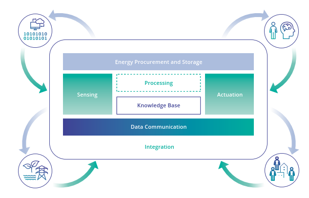
Figure 1.2.2 defines an integrated smart system showing its components and modules, while interacting with any sort of environment. Smart systems integrate sensing and/or actuation as well as signal and power/energy processing to enable actions. Smart systems utilize multi-functional perception, and are predictive, configurable, contextual and adaptive.
The Covid-19 pandemic has demonstrated the critical role that smart components, modules and systems can play for the world’s security and health. Key topics here range from an acceleration in the analysis of DNA samples, the availability of automated medical support and diagnosis tools, to tracking systems for tracing and controlling the spread of the disease, not to mention the mental and physical assistance that smart devices have provided to quarantined people through cellular networks and the internet.
The Internet of Things (IoT) is one of the main technologies enabled by smart components, modules and systems. It supports such game changers as virtual reality (VR), augmented reality (AR), extended reality (XR), digital helpers, and spread use of AI and edge computing. These elements are pivotal for optimized data collection and profitable machine-to-machine (M2M), human–machine interface (HMI) and human–computer interaction (HCI), bringing smartness to human activities (smart cities, smart transportation, smart grids, smart manufacturing, etc.) and human health and well-being (e-health, m-health, implants, ingestibles, wearables, personalized medicine, inclusion of people with a disability, etc.).
Another major application is digital industry. Smart systems harness data, extract information, distill knowledge and convert it into actions and/or provision of improved decision support. This is achieved by integrating components and modules for data acquisition and context-based actions, signal conditioning and data analysis, and by communicating elements to organize collaborative, adaptive and self-repairing networks. In offering alternative access via the cloud to data processing and knowledge extraction engines, smart components, modules and systems enable the deployment of edge computing, thus reducing the demands on communication bandwidth and system-level power consumption. However, this also creates challenges for the self-powering of edge devices of increasing complexity, and the need for such power demands to be carefully managed and limited, using ambient energies where possible. Software (SW) integrated into such devices (with the appropriate architecture for sustainable processing) needs to be considered very carefully. How, where and when data is gathered, processed and transmitted has major ramifications on the peak and average power consumption not only of the edge devices but also the gateways, servers and the cloud. The most energy efficient manner possible (based on energy sources available) should be found to maximize battery life and reliability. Having billions of connected IoT devices will increase the load on our IoT infrastructure at all levels. So, the overall architecture in inter-play between the entire system components needs to be carefully considered in terms of power, security, latency, processing capability, etc. Resolving this challenge requires not just technology advances, but also close coordination and collaboration between all the “power IoT” stakeholders based on realistic targets and expectations.
Technology advances enabled by components, modules and systems integration are as follows:
-
Greater performance and digital configurability of sensors, analogue and RF components, along with high-performance computing functions.
-
Technology integration of electronics, cellular/chemical/biochemical interaction, fluidics for multifunctional smart systems.
-
Extending pure electrical functionalities to integrated photonics by hybrid and heterogeneous photonic integration, i.e. merging different PIC technologies to compensate for missing functionality in individual cases. This requires seamless integration of electronic and photonic ICs, both at design level and technology level, which makes lower power consumption of electronic and photonic chips inevitable.
-
Embedded intelligence in the ECS, typically realized by a combination of hardware and software components, leading to higher functionality, improved interoperability, less demanding or more natural interfacing, both for machine-to-machine interfacing, human-to-machine interfacing (e.g. haptic interfaces) and decentralized signal and information processing, i.e. edge AI.
-
Greater performance in power electronics components through an impact on the thermal characteristics and higher power density and electromagnetic interference (EMI) performance of components, modules and systems.
-
Reducing energy consumption of electronic components, without decreasing component performance (e.g.., in the detection limit of MEMS/NEMS sensors), on all levels and functions: component, module and system integration, RF transmission.
-
Improving energy efficiency and energy autonomy of electronic systems through smart and intelligent battery management, energy harvesting and low leakage storage devices.
-
Improved reliability, security, safety, both at software as well as hardware-level, through self-monitoring and self-repair also for harsh environments.
-
Wearable and/or disposable smart systems with flexible and stretchable materials, through hybrid integration of traditional integrated circuits with flexible electronics.
-
Structural electronics, opening a new form of electronics integration on/in various materials, making the package an active part of the device.
-
Closer co-operation between HW and SW developers at the early concept stages (e.g. in designing configurable and context- and constraint- aware data collection and processing architectures) to ensure that, at a system level, the amount and means of processing and communications is optimized and is truly scalable and sustainable.
-
Non-fossil and biodegradable materials for greener electronics and reducing environmental impact of ECS and reduction of the use of resources in general, in materials, process energy, recycling of materials.
-
Quantum technologies, with components that harness quantum phenomena for computing, communication, imaging and sensing (e.g. superconducting or Si qubits, or ion traps), interfacing components and modules for quantum system integration, from cryogenic temperature (e.g. cryo-CMOS, superconducting circuitry) to room temperature.
-
Miniaturization of systems at all levels to increase the performance and to save resources and materials.
-
Modular systems allowing inclusion of re-used and recycled components and new high-performance building blocks for sensor-supported intelligence (e.g. sensor fusion and decision-making tasks). Including, including Digital Product Passport concepts to reduce data gaps in intercircularity and recycling.
-
Improved system engineering efficiency using highly dynamic systems supporting automated design for easy integration of new hardware or software components / modules.
Technology advances at the component, module and system level will have a key impact on applications. Future smart components, modules and systems will show a strong increase in functional and structural complexity and higher integration levels. They will show more diverse features and material integration in even smaller form factors.
Applications are the driver for such approaches:
-
Communication landscape with 5G, 6G and increasing data rates, including Non-Terrestrial Networks (NTN), time-sensitive network (TSN) as well as navigation and localization, including also optical integration, components and systems for fiber networks.
-
Autonomous systems– in mobility, transport, logistic, manufacturing or control of buildings and micro-grids, etc. (ensuring faster time response and decreasing the impact of human error).
-
Ultralong lifetime remote or difficult to access applications, e.g. structural monitoring of bridges, tunnels, civil structures requiring lower power consumption devices and supporting architectures, particularly for the autonomy of IoT devices, both energy autonomy and decision-making enabled at the edge.
-
Healthcare landscape with applications towards prevention, assisted care, Point-of-Care devices and telemedicine, including rehabilitation, disabled assistance as well as treatment.
-
Life science and pharma domain moving towards personalized medicine and regenerative medicine based on organ-on-chip technologies and smart multifunctional systems.
-
The transition in mobility towards zero-emission power trains, with their significant cost and energy efficiency challenges, including energy systems for high-power charging and/or highly variable and changing conditions.
-
Industry 4.0 manufacturing landscape to enable agility and autonomy, as well as energy and resource efficiency, including manufacturing down to lot-size-1.
-
Overall transition from stable controlled environments to harsh environments with longer operational lifetime and variable conditions.
-
Progression to scalable, fault tolerant and ultimately self-monitoring and repairable/re-configurable networks particularly for long life span applications such as structural health monitoring. Synergies with technologies such as neural networks for such adaptations should be considered.
-
Sensing of environmental parameters in smart agriculture, livestock or aquaculture, in manufacturing and working places, at home and in urban areas, e.g. for higher yield, energy efficiency and well-being.
-
Imaging applications for security, healthcare, digital industry, (precision) agriculture, food industry, digital society (television, social media) and perception.
-
Enabling repair as business, including repair index and set-up of repair processes.
Electronic components, modules and systems are versatile in terms of design, size, material and composition, and thus the network of stakeholders involved in the production process of smart systems is equally complex. Europe’s supply chain for smart systems production consists of more than 6,000 large companies and SMEs3. Emphasizing and supporting ECS manufacturing can lead to increasing smart systems activity for European industry. In the ECS sector, this means about nine million jobs across Europe.4 The European Chips Act is addressing these topics for a stronger European microelectronics value chain.5
The Covid-19 pandemic has revealed the vulnerability of global, distributed value chains. New models that will bring greater efficiency and more agile production processes need to be developed, and European manufacturing increased in key areas. This will ensure an effective and swift reaction to sudden market shocks as well as flexible manufacturing, accommodating shorter life cycles of products and fabrication-on-demand.
Europe is stronger in some microelectronic technologies, e.g. in MEMS sensors. MEMS technology is highly different in nature to CMOS, highly benefiting from heterogeneous integration. According to Yole Développement6, the global MEMS and sensor market (excluding RF filter modules) will almost double from US$48 billion in 2018 to US$93 billion in 2024. Assuming the same annual growth rate, the market should reach US$180 billion by 2030, with Europe supplying at least one-third to one-half of this market, with hopefully the same success in other microsystems markets.
Even though European microchips manufacturing market share is only around 10 % (See Figure in Chapter 1.1.4), the European share of integrated products and ECS systems is much higher, for example in the automotive or telecom sectors. Software including firmware and middleware is an important part of the ECS systems (see Chapters 1.3 and 1.4). The system houses and OEMs also often catch a higher share of value of the final product than component providers. This emphasizes the importance of integration of ECS instead of providing or manufacturing components only. ![]()
![]()
To summarize, investing in the future of electronic components, modules and systems integration has the following strategic advantages for Europe:
-
Strengthening Europe’s economy through the generation of high-tech innovations.
-
Increasing the added value in Europe by integrating more functional systems and products, e.g. in automotive, med tech and telecom industries.
-
Enabling a successful Twin Transition (Green and Digital) in an economically feasible way through multifunctional smart devices.
-
Ensuring European sovereignty and securing strategic Intellectual Property from European companies on advanced technologies in microelectronic ecosystem with regards to heterogeneous integration.
The following three Major Challenges are identified:
-
Major Challenge 1: Enabling new functionalities in components with More-than-Moore technologies.
Developing new features for sensors and actuators and smart systems via new materials and methods.
-
Major Challenge 2: Integration technologies, processes and manufacturing Integration technologies, processes and manufacturing.
Identifying the system optimum regarding the interplay between components to modules and systems.
-
Major Challenge 3: Sustainability.
Sustainable integration processes and recyclability of components, modules and systems to minimize their environmental impact
1.2.5.1 Major Challenge 1: Enabling new functionalities in components with More-than-Moore technologies
Physical and functional integration (PFI) considers the development of new elements and methods enabling more functionalities to be integrated physically on components, modules and systems, in the most effective form factor. This requires interdisciplinary technology innovations as smart components, modules and systems may utilize a combination of features based on nano-electronics, micro-electro-mechanic, thermoelectric, magnetic, photonic, micro-fluidic, optical, acoustic, radiation, radio frequency, biological, chemical and quantum principles. Furthermore, many types of devices are to be integrated together, such as sensors, actuators, energy generators, energy storage devices, data processing devices, transceivers and antennae. Different technological approaches such as mainstream silicon technologies, MEMS/NEMS, MOEMS and Large Area Electronics can be combined for the synergistic assembly of electronic and photonic devices. PFI requires not only the integration of physical components together, but also the co-design and integration of hardware and software, especially embedded software to create reliable and sustainable functional systems. This also extends to the development of architectures that enable such systems to be configured dynamically and optimally for a given application.
Physical and functional integration goes beyond the compact monolithic SoC approaches supported by the semiconductor technologies covered in the Process Technology, Equipment, Materials and Manufacturing Chapter. The challenge covers new functionalities and materials, using More-than-Moore and system in a package (SiP) technologies, where all functions are designed together to improve performance and compactness, something that also enables the heterogeneous integration of separate devices with different fabrication processes and methods. SiP is indeed a mixed arena between the previous Process Technology, Equipment, Materials and Manufacturing Chapter and this one. In the former Chapter, SiP approaches result from the natural technological evolution of back-end semiconductor processes and are mostly related to the compact hybrid/heterogeneous integration of technologically 'homogeneous' components (e.g. chiplets) while this Chapter focuses on different integration methods of components with a higher degree of technological heterogeneity in different platforms, including their Integrated Circuit carriers, such as wafer level fan-out-packages, PCB boards, printing and co-packaging of optics and electronics. This chapter concentrates on the physical integration of hardware, including computational devices into systems, while leaving the software to the Embedded Software Chapter. ![]()
![]()
Given the broad range of physical scenarios they face, smart components, modules and systems need to interact with many environments, ranging from lab to industrial and harsh environments to in-vivo.
There is a multitude of operational issues affecting smart components, modules and systems regarding energy, performance and size. With respect to energy, for portable IoT devices, there is a need for low-power operation and provision of energy autonomy (self-powered devices or devices providing short-/medium-/long-term autonomy, depending on the application) on the one hand and dealing with high-power density and thermal stress on the other. Regarding size, the optimal “minimum” size must be achieved. Heterogeneous integration and advanced packaging and interconnection technologies need to be utilized for achieving the best performance in the smallest system-level form factor. In high high-end consumer electronics, high-performance and ultra-dense compact interfaces at all integration levels are needed, from chiplets and chip assembly and packaging to component and module level connectors and connections.
MEMS/NEMS development focuses on sensors and actuators that benefit from the free surfaces and volumes that MEMS/NEMS processing is able to produce in a semiconductor substrate. The former relies on new generations of inertial measurement units (accelerometers and gyroscopes) with increased performance, with or without AI support, magnetometers, pressure sensors, microphones, as well as particle sensors; the latter rely on piezoelectric, electro-statically or electromagnetic driven micro-mirrors, print heads, oscillators (membranes and cantilevers), tunable lenses, loudspeakers and piezoelectric micromachined ultrasound transducers (pMUTs). New piezoelectric materials, such as scandium aluminum nitride (ScAlN) enable new applications and improved performance for MEMS devices, e.g. in acoustic RF filters, in optical systems such as lidars and in ultrasonic sensing. For hydrogen detection applications, existing MEMS technologies for pressure sensing are used and optimized. Additionally, new MEMS concepts for hydrogen detection are assessed to enable the future hydrogen economy.
The technical challenges for new and future integrated photonic components, modules and systems initially lie in a suitable co-design strategy (including associated methods/tools) of the various technologies to be combined as well as in their common processability and hardware integration (compatibility). The high level of integration also requires a special focus on thermal management through thermally more robust components (e.g. laser with temperature-stable wavelength), optimized thermal design, and suitable cooling concepts. This aspect, as well as other requirements, will determine the design and technology of future packages of photonic components. A particular focus is on those cases in which photonics and electronics have to work together at high bandwidths, like very high-capacity transceivers, interfaces to electronic switching circuits in communications and data systems, high pixel-count active sensors, 3D imaging and displays. Another technical challenge is the lack of standard solutions for hybrid integration. Additionally, we face a lack of standards for development (e.g. qualification testing) or even legal framework conditions (e.g. for the regular use of smart glasses and similar applications).
Heterogeneous integration technologies are strongly driven by consumer applications, such as the various types of portable and handheld devices. The manufacturers and associated supply chain for these high-volume applications are primarily based in Asia, and so for PFI Europe needs to reinforce its supply chain of integration and packaging solutions. The convergence between sensing and imaging domains for consumer applications, for example face recognition and AR based on consumer lidar solutions, requires co-integration of (high-speed) electronics and Integrated Photonics into compact systems. Further, portable consumer electronics utilize flexible structures and technologies, which aim at even thinner and more flexible electronic components and systems e.g. for displays, wearables and novel human-machine interfaces (HMI). Structural and 3D electronics enable incorporating electronics in 3D surfaces and mechanical components by means of molding, additive manufacturing or laser direct structuring (LDS). Novel flexible and stretchable substrates (such as thermoplastic polyurethane (TPU) and polydimethylsiloxane (PDMS)), as well as new materials for active components, including conductive and dielectric inks, with organic materials, metal oxides, nanomaterials and 2D materials are required for realizing new applications from touch panels to RF antennas, control electronics, embedded lighting and sensors/actuators.
One of the key application drivers for the PFI of smart components, modules and systems is the IoT and its sensor nodes, which require a wide range of sensor and actuator functionalities, combined with data processing and wireless communication, and with power autonomy provided by energy storage and harvesting devices. In many cases, power autonomy is the limiting factor in such applications. This means the development of low-power solutions for sensors and actuators, as well as radio communication components and processing. Thermal management challenges introduced by increased functionality in a minimum form factor need to be solved. New and improved energy storage, especially low-leakage rechargeable storage devices, needs to be developed as well as universally deployable harvesting solutions to improve the case-specific devices used today. In addition to this, it is important to improve in low-power techniques at the system level with co-design of hardware and software and overall system architecture, e.g. in wireless sensor networks, to ensure reliable, sustainable and energy efficient data collection and processing systems attending to the energy available and the possible processing capabilities split at the edge, gateway and cloud. Reliable and fault-tolerant wireless networks are required for applications where long-term continued sensing is critical (e.g. structural health monitoring of civil infrastructure).
Another domain strongly reliant on PFI are Electronic Control Units (ECUs). Due to their complexity and high degree of integration, these systems benefit from advances in generative design, miniaturization, scalability, increased processing power, cybersecurity, AI and machine learning integration, prognostics and health management as well as sensor fusion.
Components to provide power efficient computational resources, i.e. low-power microprocessors and devices with novel computational architectures such as neuromorphic devices, are needed, as are low-power computational methods, including distributed and low-power AI solutions in hardware, software, and in-sensor data processing. In addition, reliable, energy-efficient, scalable, low-loss interconnection and packaging solutions are a necessity.
Smart components, modules and systems leverage a multitude of materials, such as silicon and other-than-silicon semiconductors, precious and rare earth metals, ceramics, polymers, glass, inks and functional materials for sensing, actuation and energy harvesting, as well as hybrid combinations of substrates and materials (e.g. Si, ceramic, polymer, glass, metallic glass), in packages and in systems, extending the coverage of the usual materials in semiconductor-based technologies. Many of the new features required by future smart systems can only be achieved by introducing novel materials into the devices and systems, from back-end of the line processing of the microchips, or by post-processing on CMOS, to novel IC carrier technologies, including fan-out wafer level packaging and other SiP technologies as well as PCBs or in printing, additive manufacturing or other means. The development of new materials and the compatibility of those (with regard to e.g. process compatibility, environmental compatibility) is critical to the future development of PFI.
Quantum technology provides a new modality for More than Moore technologies not industrially considered earlier due to technology limitations in field-deployability, extreme cooling requirements etc. Recent years have seen rapid technological developments in the technological readiness of many quantum technologies: Quantum sensors, especially those based on gas cells, are being industrialized and miniaturized, promising better stability and accuracy of measurements, e.g. in magnetometry and inertial measurements. Quantum computers are developing into larger and more powerful machines year after year. Quantum communications, or Quantum key distribution (QKD), enable secure encryption based on quantum states of photons. The rise in the applicability of quantum technology is based on successes in materials, fabrication processes and quantum science itself, but also in major part in the successful development of enabling technologies, such as control and low-noise readout electronics, packaging and heterogeneous integration and cryogenic cooling solutions, many of which are based on the successes and processes of electronics and semiconductor industry. Hence, the further development of these enabling technologies should be considered in detail.
The following key focus areas address the multimodality of ECS, which goes beyond semiconductor technology, requiring advanced packaging and heterogeneous integration of diverse materials, components and platforms. Full coverage of the physical-functional integration requires considering both the physical integration technology platforms and the functionalities of the integrated systems.
-
Sensing, imaging and actuation:
-
Sensors and actuators leveraging the integration of MEMS/NEMS, MOEMS and micro-optics elements.
-
Sensors and actuators for biological, medical and diagnostic applications, and for sensing of human vital signs and biomarkers, as well as for selective detection of gas and volatiles, allergens, residues/pollution in food/water, atmospheric particles, hazardous substances and radiation.
-
Sensors and systems enabling integration behind OLED and sensing through the OLED display.
-
Sensors and systems for sensing and imaging in the short wavelength infrared range, based on Ge on Si Integration or Pb free quantum dots, enabling a broad range of new applications in the areas of lighting, biotechnology and life sciences, photovoltaics and information processing.
-
Advanced global shutter and rolling shutter CMOS Image Sensors (CIS) based on novel pixel technology for VIS-NIR imaging applications, with the goal to improve the performance, sensitivity, and efficiency of VIS-NIR CIS pixels, enabling high-quality imaging across a broad spectral range, as well as infrared imaging.
-
Imaging systems: lidars and radars, including multi-modal and hyperspectral, i.e. spectrally resolved, sensors.
-
Sensors and systems utilizing quantum principles, e.g. single photon sensors, including required cryogenic and cooling components and systems.
-
Devices with new features and improved performance for sensing and actuation using novel materials (metal nanowires, carbon nanotubes (CNTs), graphene and other 2D materials, cellulose nanofibers, nitrogen vacancies in diamond, metamaterials, metallic glass etc.), in combination or integrated with/on CMOS.
-
Sensor fusion and virtual sensors including appropriate data and communication infrastructure, e.g. for condition monitoring, prognostics and health management for ECUs.
-
Ultra-low power event-based sensors, e.g. inertial motion & image detection for asset tracking, incident/anomaly detection, etc.
-
Materials that ensure the hermetic sealing of sensors, actuators and systems and at the same time contribute to the miniaturization of components.
-
-
MEMS technology
-
CMOS or GaN-compatible thin film piezoelectric materials, such as ScAlN for piezo-actuated MEMS sensors and actuators.
-
Acoustic piezo-MEMS devices, pMUTs, and Acoustic RF filters for high frequencies above 6 GHz.
-
Audio MEMS devices with more advanced integrated functionality, such as integrated noise cancelling.
-
-
Integrated Photonics
-
New materials for active photonic devices, such as 2D materials, Lithium Niobate, Indium Phosphide; for improved performance, such as higher bandwidth in modulators, and detectors.
-
Light sources (e.g. lasers and laser modules) with higher power and better performance and with tunable wavelength, using external cavity on photonic integrated circuits (PIC).
-
New waveguide materials and components to expand the wavelength range from UV up to mid IR optical elements for beam shaping and manipulation (like ultrathin curved waveguides, meta-lenses, tunable lenses and filters, next generation holograms, ultra-wide-angle holograms).
-
Display technologies (like micro-LEDs, MEMS-mirrors, Phase Arrays) and sensors (e.g. for eye tracking).
-
New devices for Quantum PICs.
-
-
Flexible electronics
-
Sensing devices and power sources compliant with hybrid integration in wearables, considering flexibility, durability (e.g. washability) and biocompatibility.
-
Flexible and stretchable sensors and modules, e.g. OLED displays, OPVs, touch surfaces and other sensors/actuators, conformal antennas.
-
Functional materials for flexible and stretchable devices; organic and inorganic semiconductor materials and inks, perovskites for OPV.
-
Barrier materials, dielectrics, and transparent conductor materials and inks for flexible electronics and additive manufacturing.
-
-
Communications
-
Module-level high-speed wireless communication features, including current and new frequency bands.
-
High-speed photonics communications modules beyond 1 Tb/s.
-
New front-end components, filters and functionalities e.g. active antennas for 5G and 6G communications and non-terrestrial network solutions.
-
Low latency and low power communications in-package/module as well as at system level for the edge and IoT devices.
-
Continuous delivery of new features and fixes through Over-The-Air (OTA) updates to ensure the security of the device over time and reduce the digital waste increasing the life of a device.
-
Strategies and components for Electromagnetic interference (EMI) mitigation and reliable operation in harsh environmental conditions.
-
-
Energy and thermal management:
-
Low-power/low-loss modules for low-power sensing, actuation, processing and communication.
-
Power architectures with digital interfaces driven by dynamic and context aware algorithms that can adapt based on energy available versus needed for sensing, actuation, processing and communication.
-
Energy-autonomous multi-sensor modules and systems including energy harvesting, sensing, actuation, processing and communication.
-
Power management components and modules compatible with harsh environments (high temperatures, vibrations, electromagnetic interference (EMI) conditions for industrial, automotive and space technology).
-
Devices using non-toxic materials for efficient energy sources, storage and harvesting devices (thermoelectric, piezoelectric, tribo-electricity, etc.), and higher performing electrodes and electrolytes for improved capacity and low leakage of energy storage devices or new lightweight energy harvesters for mobility and transportation applications.
-
Solutions for thermal management for integrated photonics and RF systems at different integration levels including advanced and active cooling systems.
-
Thermal management and smart cooling systems for industrial applications and harsh environments.
-
Efficient smart compact cooling solutions and approaches for quantum devices and cryogenic multiplexing with semiconductors or superconducting devices.
-
-
Information processing:
-
Component and system-level features for self-diagnosis and module-level signal processing and control features for self-diagnosis, self-monitoring, and self-learning and self-repair.
-
Sensor level hardware and software solutions for security and privacy and data reliability.
-
Machine learning and artificial intelligence and data analysis at the sensor, module and systems level, i.e. on the edge data analysis embedded at different levels for smarter devices, including AI at sensor level.
-
Integrated and scalable solutions, both Software and Hardware integration with increased processing power for more sophisticated features, especially for edge AI and ECUs.
-
Use of quantum computing and integrating quantum computing for data-analysis.
-
1.2.5.2 Major Challenge 2: Integration technologies, processes and manufacturing
Smart components, modules and systems require a multitude of processes: silicon and other micro- and nano-processing, additive manufacturing, lamination and other interconnection and assembly technologies, as well as hybrid combinations. To increase the integration density and combine the above-mentioned features, many different integration and packaging technologies are required, such as thin film processes, embedding, classic assembly and joining methods, both for single components as well as modules.
Heterogeneous integration, from components up to the system level, requires-engineering on many technology domains, such as power, signal integrity, EMC, thermal, mechanical. All such domains and their hardware and software interplay (power and communications) must be designed together to ensure a high device and system level performance and the necessary integration. The challenge here is to combine all these domains in the design and simulation of integrated systems, often with inadequate information of all the properties of the included materials, components and processes. Where possible historical data and related algorithms should be used to predict and optimize system level performance. This may involve changing sensing intervals and/or how and where data is processed and routed. Furthermore, standardized and interoperable design and simulation methods that enable and support such multi-physics and multimodal design and manufacturing must be addressed, with possibility to parameterize not only the material parameters, but also system parameters, e.g. variability in the quality of the contact (e.g. thermal, mechanical) between the transducer and the ambient energy sources in the case of power harvesting. Modelling and design tools for thermal, mechanical and electrical characteristics in small 3D packages, including molded and additive manufacturing methods are needed, linking to Architecture and Design; Methods and Tools Chapter. ![]()
Flexible electronics is an enabler to reduce the weight, volume and complexity of integrated systems and products, to create novel form factors and 3D design features. Currently, the majority of flexible electronics products are based on polyimide (PI, Kapton), copper laminate substrates, etching of copper to pattern the circuitry, and conventional SnAgCu (SAC) soldering or anisotropic conductive adhesives (ACA) bonding processes for the assembly of discrete components on the substrate. Development towards smaller feature size in printing technologies increases the requirement of registration, or layer-to-layer alignment accuracy. Development of IC interconnection and bonding technologies especially to flexible and stretchable substrates is critical for improved performance, yield and reliability. In addition, pilot lines and fabrication facilities and capacities need to be developed.
In integrated photonics, if it comes to monolithic integration, the optical waveguides and devices are fabricated as an integrated structure onto the surface of a substrate, typically a silicon wafer. As a result of integration, complex photonic integrated circuits (PICs) can process and transmit light in similar ways to how electronic integrated circuits process and transmit electronic signals. New waveguide and active materials are constantly developed, both for monolithic integration of components, such as SiN waveguides on Silicon or Ge detectors and 2D materials for active components, such as modulators or detectors. The fabrication of PICs consists of a multi-faceted integration problem, including monolithic integration, heterogeneous integration of active components (e.g. laser sources), and high-speed driving electronics for e.g. high-speed communications above 100 GHz bandwidth, thermal management and other functionalities, such as fluidic functions for bio and medical sensing. Further system development regarding integrated photonics includes an often 3D assembly of electronics and photonics with passive optical MEMS as well as optics components like lenses, mirrors and beam splitters.
Integration and packaging technologies for quantum systems are key enablers to make quantum sensors and other systems industrially applicable. The integration and packaging in quantum technology poses several non-typical requirements for preserving the quantum coherence. Such requirements include use of non-typical materials, such as extremely-low loss dielectrics and superconductors. Further, the packaging must support extreme cooling or even cryogenic operation, either by integrating a cooler technology inside, or by being inserted in an external cryo-cooler, which also entails vacuum operation. Thermal conductivity and handling of thermal expansion of different materials at every level, from wafer and chip level integration methods, to packaging and connection to room temperature are critical. Especially quantum computing requires multi-channel high-fidelity control and read-out solutions, with accurate synchronization and timing, from low-frequency to GHz range to the optical range of frequencies, depending on quantum system modality. Cryogenic electronics, cryo-CMOS or similar, are developed for solving these requirements, at the same time increasing the integration level of the quantum system, by introducing the control and readout elements closer to the qubits or other quantum devices.
The critical requirements to enable new advanced applications are to ensure sustainable and cost-efficient manufacturing while providing optimal performance and reliability. Further important developments include integration of different silicon IC components into miniaturized multifunctional modules following different SiP approaches, combining technologies such as flip chip, bonding, lamination and substrate materials such as silicon, glass, ceramics and polymers. Multifunctional integration also requires the development of multi-domain integration – e.g. the integration of photonic and RF functionalities into smaller form factors and together with sensors and CPUs.
For many portable devices e.g. Wireless Sensors Network (WSN) edge nodes, the power source in itself becomes a more complex challenge to integrate materials and devices, moving from traditional batteries and capacitors. This requires a complex combination of energy harvesting transducers, primary and rechargeable storage devices that need to interact with PMICs, MCUs, sensors and transceivers. Collectively they need to make decisions at a node and network level on when to use versus store energy and where to take it from. The physical mounting of transducers and electrically controlling their characteristics (e.g. impedance matching) will also be critical to maximize their performance.
The challenge of integration processes, technologies and the manufacturing of smart components, modules and systems is mainly about dealing with the complexity of heterogeneous integration and scalable manufacturing technologies with different economy of scale approaches. These include “intensive” Si-like technologies, or “extensive” printing-like technologies, which under different assumptions and processing paradigms can offer cost affordability and production scalability. Apart from high-volume applications such as medical patches and RF front-end modules for 5G/6G small cells, many industrial applications can also require the availability of components, modules and systems in relatively small quantities over decades, which adds a new challenge to the scalability of manufacturing and implementation of the latest technologies.
The complexity and diversity of heterogeneous components, modules and systems substantially exceeds that of mere microelectronic components due to their multi-physics and multiple domain nature. In addition, the packages will include integrated functionalities, rather than being “passive” boards and frames. Integration and packaging methods should not compromise, but guarantee and even increase the performance of the interlaying components. Especially low-loss integration methods to enable integration of large RF systems or integrated photonics. These technologies would enable e.g. RF front ends or active antennas for millimeter wave frequencies enabling novel beyond-5G telecom solutions, or in integrated photonic communication and sensing systems. Merging different PIC technologies to compensate for missing functionality in individual cases is based on a variety of technologies, such as die flip-chipping, wafer bonding, micro-transfer printing, edge coupling, and others. Amongst current examples, one that is particularly pronounced is the integration of III-V light sources with silicon photonics, which is missing from silicon technology on its own.
In this multifunctional and multimodal integration at the component, module and system level, the development of manufacturing methods that meet the accuracy and repeatability criteria of high-quality and high-reliability products for a broad range of applications and constraints (physical, mechanical, thermal, environmental) is challenging and needs development. This method development shall be accompanied by process modeling leading to a digital twin for manufacturing allowing documentation, simulation and improvement of manufacturing challenges in a digital environment. (see also Chapter 2.4)
Additive manufacturing can provide structural and functional solutions for smart components, modules and systems integration that are not feasible with traditional methods. These methods will enable zero-defect manufacturing starting at lot one. Although additive manufacturing also improves manufacturing flexibility, solutions for the cost-efficient scaling of these fabrication methods must be addressed. 3D component, module and system integration methods will need to be developed to provide greater functionality and miniaturization in a cost-effective, sustainable and scalable way.
With respect to this multi-modality of heterogeneous integration methods, the key focus areas are divided based on the main technologies: advanced packaging and SiP technologies, integrated photonics, flexible electronics, quantum systems and manufacturing methodology as follows.
-
Advanced packaging and SiP technologies
-
Robust heterogeneous 3D integration of sensors, actuators, electronics, processing units, communication, RF front-end components and energy supply into miniaturized systems.
-
Embedding of power sources (energy harvesting transducers, batteries, supercaps, etc.) into a package (PwrSiP) and on a chip (PwrSoC).
-
IC carriers with integrated voltage regulator and capacitance increasing the power delivery efficiency, as well as finer structuring in IC carriers: below 5/5µm line width and spacing and finer micro-vias (below 15µm diam.).
-
Multi-node chiplets for compute applications involving high speed chip-chip interconnections with high resolution electrical and optical routing in substrate or redistribution.
-
Integration with biological and molecular systems, including fluidics and surface coatings and functionalization materials and methods for multi-functionality on the same base structures, e.g. biosensor arrays on Silicon.
-
New functional materials for packaging that enable integration of sensing or other functionality or enhanced functionality into the packaging itself, e.g. packaging as a part of the antenna or sensor functionality, e.g. embedded heatsinking/spreading to increase the thermoelectric energy harvested.
-
New materials and methods for housings and coating features and new substrate materials for specific requirements: high power, high frequencies, disposable, bio-compatible, non-fossil, harsh environments.
-
Rapid prototyping and manufacturing technologies (additive manufacturing, 2D and 3D additive technologies, etc.).
-
High-performance materials for passives enabling close coupled passives for high-density heterogeneous integration such as magnetic cores, high-k dielectrics.
-
Ultra-dense and small interfaces in all integration levels, from chip assembly and packaging to component and module level connectors and connections.
-
Integration of different sensors and sensor hubs for sensor fusion (e.g. combination of acceleration sensor, microphone, microspeaker for enhanced noise cancellation).
-
Manufacturing and characterization processes for hermetic sealing of components or subsystems with low leakage level.
-
-
Integrated Photonics and co-integration with electronics
-
Photonic-electronic system integration based on integrated photonics, including high-speed RF electronics, MEMS/NEMS sensors, etc.
-
Multi-domain electro-photonic integration and electro-optic co-packaging.
-
Wafer-level integration of photonic and electronic components for smart emitters and detectors.
-
Enabling electronic-photonic systems by heterogeneous integration of active components on PICs (III-V semiconductors, ferroelectrics, ultra-low-loss waveguide materials).
-
Heterogeneous integration processes and equipment for integrated photonics, including high-precision component placement and bonding, as well as low-loss fiber coupling to PICs.
-
Quantum PICs: Integration of single photon detectors and sources and quantum photonic system in PICs.
-
-
Flexible electronics
-
Integration towards low vertical form factor (<100 μm) and the miniaturization of external matching networks through integration.
-
Submicron LAE fabrication processes and equipment (printing technologies in general, nanoimprinting, reverse offset printing, etc.) and automated manufacturing equipment for flexible electronics, including testing tools for electrical and non-electrical properties.
-
Interconnections processes and tools for flexible and stretchable devices and structural electronics (in glass, plastics, laminates, etc.).
-
New/alternative non-fossil, organic, biocompatible and compostable substrate materials for e.g. implants, ingestibles, wearables, biosensors.
-
Adhesives, bonding materials and methods for integrating chips on flexible substrates.
-
Use of flexible Si-substrates for 3D form factors and for flexible electronics.
-
Integration and embedding of diverse materials and components such as antennae, PV panels, energy storage devices, magnetics, interconnect, heatsinks, displays, etc in flexible or conformal electronics.
-
-
Quantum systems
-
Materials and methods for integration and packaging of semiconductor electronics, Integrated Photonics and superconducting devices at cryogenic temperatures, including 3D technologies.
-
Integration and interfacing and cabling solutions for combining room temperature systems and cryogenic quantum components, sensors and systems.
-
Integration methods that enable scaling quantum systems efficiently, from wafer level 3D integration to module and system level.
-
Cryogenic electronics, cryo-CMOS and similar for increasing the integration level of quantum systems and enabling scaling up of quantum systems.
-
Development and miniaturization of cryogenic cooling systems, e.g. solid state coolers.
-
-
Manufacturing methodology, characterization and testing
-
Automation and customization in component, module and system integration for large-scale manufacturing, including Industry 4.0 techniques, design for manufacturing based on production data techniques, and lot-size-1 manufacturing, e.g. BIST (built in self test) capability of components.
-
Manufacturing and testing tools (including tests, inspection) for components, modules and systems, enabling zero-defect integration.
-
Process modeling approaches with focus on productivity, yield, trustability, distributed manufacturing.
-
Material properties database for simulation and reliability based on a standardized ontology.
-
Design of new materials from properties requirements by the means of Materials by Design, materials genome and digital design approach.
-
Energy effective joining methods, e.g. low temperature soldering; selective heating processes (i.e. inductive or reactive) to limit overall temperature impact to system while packaging.
-
Self-powered embedded sensors for ongoing performance and condition monitoring and tracking of devices , e.g. for provenance, life cycle assessments, field failure analysis, authentic validation.
-
1.2.5.3 Major Challenge 3: Sustainability
In 2019, world-wide e-waste exceeded 50 million tons, and is forecasted to grow to 70 million tons in 20307. The European Union is one of the most advanced actors in e-waste recirculation processes. Indeed, in this region 42.5% of e-waste is documented to be collected and recirculated as product or component or recycled as material, whereas this is the case for only 9.4% in Americas and 11.7% in Asia. This can be explained by the clearer European and national political support for such initiatives. (Source: NU/UNITAR SCYCLE – Nienke Haccoû)
However, as increased integration will cause the borders between components, modules and systems to become blurred, and more diverse and complex materials are used at each level, the dismantling of systems into their constituent components at the end of their useful life will become increasingly difficult. Many industrial ECS products have lifetimes extending to decades, thus the environmental regulations for recyclability cannot be known in detail by the time of product design. Nevertheless, early consciousness on the issue should preside the start of the product cycle. Based on identified challenges, regulatory measures under the Eco-design Directive are intended to establish design for energy efficiency and durability, repairability, upgradability, maintenance, reuse and recycling. The European Commission presented its new Circular Economy Action Plan (CEAP) in 2020 to limit waste generation and encourage recycling, product repair and reuse. Part of this initiative is the digital product passport (DPP), which informs end-customers and businesses about products’ sustainability. In general, the concept of the circular economy (CE) builds upon well-implemented strategies to prevent waste generation and includes eco-design rules during product design phase and measures for re-using products and components after a use phase.
The European Platform on Life Cycle Assessment (EPLCA) includes information on the Product Environmental Footprint (PEF) and Organization Environmental Footprint (OEF) methods as a common way of measuring environmental performance (EU Commission Recommendation 2021/2279). The PEF and OEF are the EU‘s recommended LCA-based methods to quantify the environmental impacts of products (goods or services) and organizations.
ECS should produce smart systems not only as an enabler for, but also as an element of the circular economy, considering the sustainability of the ECS value chain and the products themselves. Focus should be on the sustainability of the component, module and system production, including processes, materials and maintenance during the primary lifetime. The recyclability of the product must already be considered in the design and manufacturing phase to enable repairability, upgradeability, reconfigurability, extension of lifetime, and re-use in a second life application, and finally the recovery of components and materials for recycling.
Given the increasing burden of improperly dealt with e-waste and considering that a significant part of CO2 emissions arises from the fabrication of the ECS themselves, extending product lifetime is important for reducing ECS-related environmental load. This needs to be addressed by designs that enable repair or replacement of faulty components, avoiding the replacement of the full module or system. To fight obsolescence, hardware and software upgrades should be supported, even in field conditions. Reducing CO2 emissions during the lifetime of the system requires minimizing the power consumption at component, module and system levels while in operation by using low-power hardware and software technologies.
For increased sustainability of ECS, the circular economy, with its 9R framework (Refuse, rethink, reduce, reuse, repair, refurbish, remanufacture, repurpose, recycle and recover) and eco-design, are the main tools to reduce the environmental footprint of ECS. Life-cycle assessment as a framework will be used for identifying hotspots and checking results of the intended reduction. But ECS themselves can also be regarded as an enabler for a more circular economy.
Future ECS products must be environmentally friendly, covering all aspects from materials, manufacturing, operation and maintenance during their lifetime, considering recycling at their end-of-life. Activities must start by ensuring circularity (eco-design, environmentally friendly materials and manufacturing), employing a low CO2 footprint over the whole life cycle, and facilitating the transition to a circular economy, wherever possible. Outcome activities will address:
-
Non-fossil, recyclable, biodegradable and compostable materials, without releasing any dangerous materials or having other negative impact on the environment.
-
Eco-design including eco-reliability of sustainable and more modular ECS.
-
Sustainability and reducing energy consumption and environmental footprint of the manufacturing and integration processes.
-
Increasing energy efficiency of ECS, during manufacturing and lifetime, and end-of-life.
-
Upstream considerations and design for repair, upgradeability, dismantling, materials separation and recycling, lifetime extension and system health monitoring, self-monitoring and healing.
-
Performance and condition monitoring, traceability, (predictive) maintenance, repair, upgrading, reconfiguring, recharging, retrofitting and re-use in second life, including ecosystems and tools to support these actions.
-
Product indexes and digital product passports for ECS.
-
Enablement of novel sustainable business models.
The development of integration processes based on new design tools will allow the dismantling of components, as their recycling and recovery of materials (urban mining) is essential. Therefore, system design techniques move towards eco-design where we need to rethink the use of multifunctional components and modules. Design for component separation and recyclability is generally required in the selection of materials and the integration technologies. Recycling technologies, as well as new approaches to second life of ECS and re-use in new applications, must be advanced. For example, with the electrification of cars, the recycling and re-use of battery packs, modules, and individual cells, and finally, materials recovery from the cells, becomes more and more important. Finally, we should of course minimize the number of batteries we use and dispose and improve recycling of batteries and battery materials.
The use of new environmentally friendly, recyclable and non-fossil materials (or compostable/biodegradable materials) must be seriously considered to replace existing materials with low recyclability in the near future. The use of these materials can easily be extended to other parts of the system, and the development of biodegradable materials can also contribute to solving the problems of recyclability. Life cycle assessment (LCA) should be used as a design tool to minimize the ECS carbon and environmental footprint, considering the full life cycle and end-of-life.
-
Eco-Design of ECS to promote circularity:
-
Use of replacement materials to comply with Restriction of Hazardous Substances Directive (ROHS) regulations (such as lead, mercury and other metals, flame retardants and certain phthalates, PFAS) and minimization of critical raw materials (CRM) dependence, including rare earths replacement for magnetics, inductors and power integrity.
-
Use of recyclable, biodegradable, compostable, non-fossil materials from sustainable sources in combination with the development of efficient and environmentally benign recycling techniques in accordance with the legislative agenda.
-
Less materials for higher functionalisation.
-
Assessment of the environmental impact of ECS at the design stage, as a tool for sustainable ECS, using life cycle assessment (LCA) or similar framework.
-
Certified up-to-date data for LCA, PEF, PCR and EDP.
-
Development of design, fabrication, integration, recovery, reconfiguration/reuse, repairability and disassembly strategies for products (module dismantling, component recycling, material recovery) and also short-lifetime devices (e.g. single-use medical devices, radio-frequency identification, RFID, tags and printed sensors) to meet the existing and emerging regulatory requirements.
-
Improvement of system reliability as a means to guarantee and extend the lifetime of electronic products with the final objective of responding to material efficiency requirements and providing an optimal balance on a life cycle scale.
-
Increasing power efficiency of ECS during lifetime by using low-power techniques with context awareness or energy harvesting.
-
Extensive use of software to increase the sustainability of ECS by extending product lifetime through continuous optimization and adaptation, by making existing ECS more intelligent through the use of AI, in particular at the Edge, and by optimizing the resource usage through hardware and software co-defined strategies. Ensure the trustworthiness and reliability of the ECS, including its software components, with a special attention to approaches involving AI that must be secure, reliable and automatically and autonomously adapted.
-
Promote methodologies allowing for the co-design of ECS hardware and software involving simulations and realistic models, including AI-aided development tools, to continuously estimate key metrics. This must be complemented by instrumentation of the ECS hardware and software to continuously assess the achievements of the key figures of merit over the entire ECS lifetime (including shelf and post-decommissioning).
-
-
Sustainable manufacturing of ECS:
-
Explore the extension of additive manufacturing methods, such as printing, that consume less resources (energy, materials, water) and are compatible with renewable materials, such as bio-based substrates. At the same time, additive manufacturing offers new design capabilities for circular, thin and flexible devices, even for single use (e.g. wearable electrodes) with specified end-of-life management.
-
Optimization of resources and processes in production environments with potential in-situ re-use and regeneration of base materials and chemicals.
-
Reduce energy consumption (and greenhouse emissions) in cleanrooms through the use of renewable energy sources and energy-efficient technologies or tools.
-
Increase water reusage in electronics manufacturing facilities.
-
Improve gas abatement systems.
-
Breakthroughs and development in recycling processes and solutions for energy storage components, such as batteries.
-
-
Sustainable products and business models:
-
Encouraging sustainable supply chains.
-
Introduction of product category rules and product indexes (including info such as energy and resource efficiency, durability, reusability, upgradability and repairability, presence of substances that inhibit circularity, recycled content, remanufacturing and recycling, carbon and environmental footprints, expected waste generation and information requirements) for components and systems to encourage the use of LCA based environmental product declarations.
-
Digital product passports should be promoted, tested and then widely established.
-
Encourage new business models to see value in eco-design and recyclability.
-
Value repairability: An EU-wide repair index inspired by the French repairability index.
-
Condition monitoring for usage as well as for health/performance and anomaly detection.
-
Improve efficiency of e-waste recyclability by robotics, thereby increasing new value streams and business through reuse.
-
The following tables illustrate the roadmaps for Components, Modules and Systems Integration.
| Major Challenge | Topic | Short Term (2024-2028) | Mid-Term (2029-2033) | Long Term (2034 and beyond) |
|---|---|---|---|---|
|
Major Challenge 1: Enabling new functionalities in components with More-than-Moore technologies |
Topic 1.1: Sensing, imaging and actuation |
|
|
|
|
Topic 1.2: MEMS technology |
|
|
|
|
|
Topic 1.3: Integrated photonics |
|
|
|
|
|
Topic 1.4: Flexible electronics |
|
|
|
|
|
Topic 1.5: Communications |
|
|
|
|
|
Topic 1.6: Energy and thermal management |
|
|
|
|
|
Topic 1.7: Information processing |
|
|
|
|
|
Major Challenge 2: Integration technologies, processes and manufacturing |
Topic 2.1: Advanced packaging and SiP technologies |
|
|
|
|
Topic 2.2: Integrated Photonics and co-integration with electronics |
|
|
|
|
|
Topic 2.3: Flexible electronics |
|
|
|
|
|
Topic 2.4: Quantum systems |
|
|
|
|
|
Topic 2.5: Manufacturing methodology, characterization and testing |
|
|
|
|
|
Major Challenge 3: Sustainability |
Topic 3.1: Eco-design of ECS |
|
|
|
|
Topic 3.2: Sustainable manufacturing of ECS |
|
|
|
|
|
Topic 3.3: Sustainable products and business models |
|
|
|
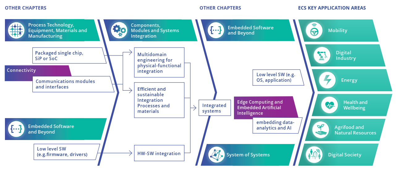
Smart components, modules and systems are key elements in a wide range of activities relevant to all Application Chapters. Conversely, the new and advanced applications described in those chapters will also give rise to new functionalities and further advances in integration technologies. Most components, modules and systems integration is based on devices developed with techniques described in the Process Technology, Equipment, Materials and Manufacturing Chapter. Furthermore, simultaneous development and co-design is necessary with Embedded Software and Beyond technologies to ensure integration with hardware and software. ![]()
![]()
The cross-sectional technologies link to components, modules and system integration in many ways. Connectivity solutions are needed for networked systems. Edge Computing and Embedded Artificial Intelligence needs to link into integrated systems for AI on the edge and on sensor level already. Quality, reliability and cybersecurity methods are paramount for ensuring reliable integrated systems. For successful multi-modal integration of electrical, thermal, and mechanical properties in integrated systems, advanced simulation methods and design tools are required, which is covered in Architecture and Design: Methods and Tools. ![]()
![]()
![]()
Thus, the field of components, modules and systems integration draws upon key enabling technologies and integrates knowledge from many disciplines. In addition, integration bridges the gap between components, modules and functional, complex systems. As the development of smart components, modules and systems will benefit from progress in all other technological disciplines, the synergies should not only be in the multidisciplinary development of the technologies, but also in the building of ecosystems (people and infrastructure). This is where all stakeholders can guide and influence each other and collaborate to assist in the development of optimized system- and application-oriented solutions.