
0. Introduction and Overview
0.1
We are living in a period characterised by unprecedented challenges: trade and geopolitical tensions, climate crisis and ageing population, to name a few. In particular, Electronic Components and Systems (ECS) bear the promise to be key tools to allow us to overcome many of the aforementioned challenges. However, faced with a flurry of possible technology options, and limited financial and human resources, Europe needs to make sure that it aligns its research efforts and public support where it can best leverage its strengths and mitigate its weaknesses, both now and in the future.
This is the purpose of this ECS Strategic Research and Innovation Agenda (ECS SRIA), jointly developed by the experts of the European ECS community, coordinated by the three industry associations: AENEAS, INSIDE Industry Association (formerly ARTEMIS-IA) and EPOSS. This ninth edition identifies the Major Challenges, necessary RD&I efforts and expected outcomes. The technology domains addressed range from micro- and nanoelectronics, smart electronics system integration (e.g. chiplets) via embedded and cyber physical systems to complex system of systems integration. It is an essential tool to drive the ECS research and innovation efforts in Europe with the ultimate goal of creating value, growth, jobs and prosperity.
ECS are the key technology, enabler and differentiating factor behind all mass applications and their innovations, serving a market of over 61 trillion Euro (see figure 0.1). Therefore, a very broad scope in the applications, in the design, the underlaying technologies, the requirements and in the manufacturing is addressed in this document, resulting in the identification of 71 Major Challenges.
They are frequently interdependent – they influence each other, become increasingly demanding, and have an impact on many areas, including technology innovation, industrial competitiveness, security, safety, business and environmental sustainability, society, etc. From this perspective, and as shown in the major challenges table in Appendix B, the Major Challenges represent key factors for the achievement of five Main Common Objectives, which are aligned with the European Commission’s strategic priorities:
- Boost industrial competitiveness
- Ensure EU digital autonomy
- Establish and strengthen sustainable and resilient value chains
- Unleash the full potential of intelligent and autonomous ECS-based systems
- Enable the ECS Engineering Ecosystem
The SRIA is developed collaboratively by numerous technical experts from industry and academia, each contributing perspective shaped by their respective background and industrial areas of interest. Its purpose is not to prioritize specific areas of the electronics components and systems domains or individual research and innovation activities. Rather, it reflects a holistic view and collective vision for advancing electronics-based industries in Europe as a whole and along complete value chains.
The three authoring industry associations — AENEAS, EPoSS and INSIDE — , which together represent the whole European ECS R&I community, are committed to identifying and discussing intersections between political priorities and the broad spectrum of activities pursued by their members.
Investing in the Research and Innovation topics described in this document will not only translate into a more competitive and sovereign European ECS value chain, but it will also boost European industrial competitiveness across all sectors.
Electronic components and systems, by their inherent nature, are the result of interdisciplinary research and engineering. These require competencies in diverse technology domains, including process technology, equipment, materials and manufacturing, electronics, and embedded software, as well as cross-sectional technologies such as edge computing, artificial intelligence, high-speed connectivity, and cybersecurity.
As a result, ECS research needs to be interdisciplinary to benefit from the multiple available sources of innovation, as well as research-intensive and market-oriented. This will ensure forthcoming ECS innovations will be of strategic value for Europe and boost its industrial competitiveness in all its value chains, and help building the strong industrial base essential for European strategic autonomy.
With the Chips Act, the Key Digital Technologies Joint Undertaking (KDT JU) has transited to the Chips JU, with a mandate extended to capacity building activities and related research and innovation activities of four operational objectives of the Chips for Europe Initiative, as set out in the Chips Act article 4:
- building up advanced design capacities for integrated semiconductor technologies;
- enhancing existing and developing new advanced pilot lines across the Union to enable development and deployment of cutting-edge semiconductor technologies and next-generation semiconductor technologies;
- building advanced technology and engineering capacities for accelerating the innovative development of cutting-edge quantum chips and associated semiconductor technologies;
- establishing a network of competence centres across the Union by enhancing existing or creating new facilities.
All the new initiatives introduced by the Chips Act have been conceived to boost European competitiveness in the ECS market and ECS-based application domains, guiding investments and resources towards strategic areas of semiconductor technology that are most critical for the European industry's competitiveness. This SRIA contributes to the identification of these critical areas and of the associated challenges that will characterise their development in the next ten years. The role of the SRIA is fundamental to identify the key starting points for RD&I and to setup multi-annual synergies with the pilot lines that will focus on more mature prototyping. The SRIA will also potentially provide the elements for the “first-of-a-kind facilities” envisioned by Pillar 2: the synergies between these three steps represent the key strategy to increase European capacity building, to boost competitiveness, and to anticipate, prevent and effectively manage future crises.
The benefits for European strategic autonomy of the development of innovative ECS technologies focused on security, safety, reliability, dependability and privacy will be discussed in the section “strategic advantages for the EU”. European technology-based, secure, safe and reliable ECS, combined with European AI solutions, are critical to securing global leadership and strategic autonomy in key areas such as Information and communications technology (ICT) and to ensure compatibility with EU values.
These innovative technologies will simplify the implementation of the European Strategy for Data1,2, and ensure security, privacy-by-design and strategic autonomy all along the industrial and digital value chains.
Threats to Europe’s strategic autonomy are to be found in the microelectronics value chain, and then downstream in the component user segments of the electronics industry. In this context, the Major Challenges identified by the ECS SRIA will help develop innovations in secure, safe and reliable ECS technologies for creating EU-based/-made solutions in the key European application domains of:
- Aerospace, defence, security.
- Automotive, transportation.
- Machinery, robotics, electrical equipment, energy.
- Communications, computing.
- Energy generation, distribution and grids
- Healthcare and well-being
and other domains.
The Chips Act aims at consolidating and strengthening European strategic autonomy, extending and boosting the KDT with a new specific focus on the upstream of the ECS value chain. Reducing the dependency on non-European suppliers and avoiding future shortages represent the main steps towards strategic autonomy: reaching the independence on non-European suppliers for critical ECS is crucial to ensure European industries and key application domains to have a stable supply of semiconductors, even during future global disruptions or geopolitical tensions. Technological leadership and strategic autonomy are the primary ingredients required to:
- Control ECS manufacturing to produce solutions designed to meet stringent security requirements; an essential aspect for maintaining secure digital infrastructures and key applications (e.g. automotive, defence, energy, etc.).
- Ensure resilient supply of semiconductors produced in Europe to support the resilience of critical infrastructure, including energy, transportation, and healthcare systems, which rely on advanced chips.
- Achieve a greater control over the technology infrastructure that underpins the European digital economy, ensuring that critical data and systems remain under European jurisdiction.
- Enhance Europe's economic competitiveness, leading to the creation of high-tech jobs, stimulating innovation, fostering economic growth, and making Europe less dependent on external economic forces.
European strategic autonomy will also require the sustainability and resilience of the entire ECS value chain since the development of innovative technologies focused on sustainability and the Green Deal will support ambitions to achieve a green, resilient and competitive Europe.
Moreover, the serious effects of climate change that we are experiencing daily and the current geo-political situation, which highlights our dependency on non-European fossil energy providers, further reinforce the need for Europe to accelerate its transition to climate neutrality by 2050.
This challenge must be perceived as an opportunity to create a new environment for boosting innovative aspects of technology and business models through achieving the following:
- Relying extensively on ECS-based technologies and digitalisation as key factors for lowering our global energy footprint at all levels of the economy, and by placing sustainability at the heart of combined digital and green transitions.
- Positioning the European players in hardware as front-runners in sustainability to secure a wider market so they can become world leaders. This will need European companies to consider the circular economy, new market positioning (by turning small market shares into specialisation areas), the environmental impact of global manufacturing, etc.
- Establishing this carbon-neutrality challenge, based on a close link between the digital and green transitions at the core of future funded collaborative research and innovation in ECS. This will help ensure a positive impact for each stage of the value chain, and achieve carbon neutrality right down to the final application/digital service.
Even in a changing geopolitical context, climate change remains an environmental and economic imperative that cannot be ignored.
Advances in ECS technologies are both a major enabler of the Green Deal for all ECS-based application fields, and a direct contributor through their significant impact on power and resource consumption of ECS manufacturing and use.
Furthermore, the strategic autonomy introduced by the Chips Act contributes to economic sustainability and security, through a reduced dependency on non-European suppliers, an increased production capacity, more competitive manufacturing processes and products, a resilient supply chain, circular economy promotion, etc.
ECS must have intelligence and autonomy capabilities to control their complexity more efficiently and more cost-effectively. This will help provide novel advanced functionalities and services, limit human presence to only where it is strictly required, improve the efficiency of vertical applications, etc. Intelligence and autonomy are also required for the role of ECS in the application domains, representing an important factor for the sustainability and resilience of the value chains: an ECS-based system that provides intelligent energy management, relying on technologies such as AI, represents a key building block – for example, for smart home and energy applications. Moreover, it also improves the resilience required to ensure optimal energy consumption in critical conditions and contributes to the sustainability of the value chain associated with vertical applications, since it reduces operational costs and environmental impact, improves the quality of service (QoS), return on investment (ROI), etc., thereby strengthening the global competitiveness of European companies and helping to achieve the objectives of the EU’s Green Deal.
With an innovative and strong semiconductor industry Europe can improve its competitiveness in the global AI landscape, and this will contribute attracting AI talent, companies, and research initiative in Europe. Supporting the key focus areas identified in the SRIA will be crucial to consolidate the European future position in the AI market and contribute to the supply chain resilience, supported by a robust semiconductor industry in AI hardware. Boosting the RD&I activities described in Chapter 2.1 of this SRIA will ensure a solid support for all the vertical domains covered by the Application chapters.
Modern ECS-based systems are too complex to deliver reliably without a coherent end-to-end engineering ecosystem that spans requirements, architecture, design, verification and validation, deployment/commissioning, operations and remote maintenance, and eventually recycling and evolution. Establishing such an ecosystem—grounded in systems-engineering best practice—improves quality, reduces time-to-market, and enables confident scaling from components to complex systems and systems-of-systems.
This objective promotes lifecycle integration through model-based and data-centric methods (e.g., MBSE and an unbroken “digital thread”) so that product information, analyses and decisions remain consistent from concept to field operation—benefiting especially SMEs that struggle to connect tools and processes. It also supports interoperable toolchains and open interfaces that enable co-design across edge–to–cloud computing and emerging modular hardware (e.g., chiplets), and aligns engineering workflows with design-platform concepts that provide shared access to IP, PDKs and design automation in secure environments.
Security, safety, reliability and sustainability are treated by design. Engineering processes should incorporate established cybersecurity and functional-safety lifecycles and requirements so that risks are managed systematically from early architecture through maintenance. Lifecycle-integrated verification, continuous assurance (including software updates and AI-assisted engineering), and traceability strengthen dependability across domains.
Delivering this objective also depends on human capital: Europe needs coordinated education, up-/re-skilling, and hands-on training pathways that match real engineering workflows across the semiconductor and ECS supply chains. (Multiple recent European analyses highlight the skills gap and the need for joined-up action by industry, academia and governments.)
In practice, Objective 5 will:
- impact industrial competitiveness by simplifying life cycle management, and improves the quality of the engineering process, making it more cost-effective and agile.
- simplify and improve the development of trustworthy ECS technologies, products and applications.
- support sustainability and resilience that reduce lifecycle management costs, as well as ensuring the automation and continuity of operations.
- unleash the full potential of intelligent and autonomous ECS, which requires completely new approaches to engineering, design and development methodologies, as well as toolchains and tools.
- improve professional training and education by strengthening and developing new and specific skills.
By consolidating these capabilities, Europe will simplify lifecycle management, raise engineering quality and agility, and reduce cost and risk—thereby amplifying the impact of Objectives 1–4.
The importance for Europe of the ECS ecosystem is twofold: On the one hand, it is a major contributor to European economic and political strength, due to its economical weight in terms of employment and wealth creation, and its contribution to European economical sovereignty. On the other hand, ECS bring benefits across many - if not all - aspects of our daily life.
Globally, the long-term market trend for electronic components is expected to exceed US $1,000 billion by 20303. In Europe, the semiconductor ecosystem employs some 250,000 people, with 2.5 million in the overall value chain of equipment, materials, semiconductors components, system integration, applications and services – mostly in jobs requiring a high level of education.

The demand for chips is expected to double by 2030, driven by the digitalisation of society and the pervasiveness of Artificial Intelligence.

Given that in the next decade, 85% of overall global growth is projected to take place outside the EU4, it is essential that the EU maintains and increases the worldwide competitiveness of its electronics component industrial ecosystem. In turn, this increased competitiveness will stimulate all the ECS value chain and downstream industries that depend on it, including transportation, healthcare, energy, security, and telecommunications, to name a few. It is a key ingredient to maintain manufacturing as the backbone of the European economy, to guide further digitalisation of society and industry, ensure Europe’s sovereignty and resilience against crises situations, facilitate the digital single market, maintain employment and move towards a better, smarter society.
Even though the European microchips manufacturing market share is only around 10 %, the European share of integrated products and electronic systems is much higher, for example in the automotive and telecom sectors. Many European companies master specialties technologies, including integration of those technologies into smart systems, combining hardware and software - including firmware and middleware -, which allow them to grab a relatively high share of the end-product value.
Systems-of-systems6 (SoS) and their formalisation were originally conceived and studied in the defence domain, but they are (and will be) vital infrastructure for many other vertical domains. For example, the shift in the mobility sector towards electrification and autonomous mobility necessitates the adoption of systems-of-systems in e.g. vehicles and roadside infrastructure. Given current and future expectations of the market, investment in SoS research and innovation7 is essential to European leadership in the mobility sector. Likewise, to remain at the state-of-the-art in embedded systems architecture and software Europe should continue to invest in this domain, despite fierce competition. From this perspective, the convergence between AI and edge computing - embedded intelligence - should be a top priority.
Europe is also internationally known for its high-quality products. European engineers are highly skilled in systems engineering, including integration, validation and testing, thus ensuring system qualities such as safety, security, reliability, etc, for their products, using development and test tools and frameworks enabling them to ensure these qualities in an effort- and cost-efficient manner following international and European standards. The EU has a robust and reliable safety and product liability regulatory framework, and a rigorous body of safety standards, complemented by national, non-harmonised liability regulations. This ability to provide high quality products at affordable costs has led to trustworthiness with customers on the one hand and increased competitiveness on the other hand, which have been big success factors for European embedded systems in almost all industries.
Europe should take benefit of its specific strengths, and of its ambitious plans - such as the “European Green Deal” - to make its ECS industry even more sustainable and competitive producing trustworthy products.
Sovereignty
European strategic autonomy in ECS calls for further collaboration between European companies and organizations. Design frameworks, reference architectures and integration platforms will lead to new design ecosystems. Integration platforms8 will provide the opportunity to leverage a high number of small and medium-sized enterprises (SMEs) and larger businesses into a platform-based economy mirroring the existing highly successful platforms of, for example, Google and Apple.
The above holds in particular for EDA Design Platforms, where global, non-European players like Synopsis and Cadence rule an overwhelming part of the market and thus de-facto control if, where and by whom such ecosystems can evolve. Providing European alternatives for such platforms will support technical enhancements e.g. the development of edge AI, embedded AI and embedded computing chips, support of the Open-Source Hardware Community (i.e., RISC-V), and many others. It will also facilitate the development of ecosystems, e.g. allowing to have a one-shop entry for start-ups/SMEs and academia to validate their innovations, novel emerging technologies and new architectures into silicon, providing non-differentiating IP’s, tool support, and a coherent design environment.
The Green Deal objectives will further drive the production of renewable energy and the large-scale adaptation of (bi-directional) battery electric vehicles, digitalization & electrification of industry, storage systems, even more local renewable electricity generation and the conversion of heating to heat pumps. Basis for the transition are along the European value chain leading edge technologies and system expertise in power electronics, control and securely connected energy systems. Consequently, Europe will have to modernize its energy grid towards a highly dynamic, blackout-protected energy infrastructure, also significantly reducing the dependency on imported fossil fuels.
Advancements in ECS, particularly in edge AI computing and in mastering the integration task into its products, will substantially contribute to enabling European Industries to build systems with guaranteed quality properties. Europe’s strengths in creating trustworthy dependable systems by high-quality system design (“made in Europe” quality) contributes to European strategic digital autonomy.
Resilience
The current geopolitical situation in combination with the aftermath of the Covid-19 pandemic is revealing increased vulnerability of global, distributed value chains, with a disturbing and costly impact on society. In order to mitigate the impact of value chain disruptions it is essential that strategic industrial ecosystems like the semiconductor sector receive the backing from the EU as well as its member states9. This means reviewing and simplifying industrial policy instruments—such as the Chips Act, Important Projects of Common European Interest (IPCEI) and Critical Raw Materials Act—to incentivize cross-value chain cooperation and accelerate European leadership in strategic technologies. These simplified policies should support the urgent need for Europe to reduce dependencies, expand its presence across the technology stack and improve competitiveness.
As stated in the Draghi report10, investing in innovation is a necessary precondition to increase productivity and thereby contribute to competitiveness. New manufacturing models that will bring greater efficiency and more agile production processes need to be developed, and European manufacturing must be strengthened in key areas. This will ensure an effective and swift reaction to sudden market shocks as well as flexible manufacturing, accommodating shorter life cycles of products and fabrication-on-demand. Again, ECS innovations will play a key role here.
In semiconductor manufacturing specifically, Europe can reinforce its lead in semiconductor processing and packaging, equipment and smart systems based on the priorities set out in this ECS SRIA. The first and second IPCEI on microelectronics, for example, have been a successful step towards strengthening European semiconductor manufacturing in strategic areas where large-scale subsidies in other regions have started to threaten the position of European players. The European Commission has set ambitious targets11 in its ‘Digital Compass’ to double the ’cutting-edge semiconductor’ manufacturing share in Europe in 2030 – to maintain strategic autonomy, and to be involved in AI and other key technologies of the digital world.
Further, the EU can work with national governments and companies to create a true European foreign economic policy, to coordinate trade agreements and investments with external countries. In parallel, the EU should create clear incentives to cooperate more easily, and develop reliable societal emergency infrastructures. This will make European societies better prepared to deal with emergency and crisis situations.
The European electronics industry is currently facing a skill gap. The European Chips Skills Academy (ECSA) estimates that the EU semiconductor ecosystem employed ~382,200 people in 2023 and, with production ramp-ups, could see ~250,000 job openings by 2030 (new roles plus replacements). Yet the graduate pipeline is projected to grow by only ~1% CAGR, yielding a talent shortfall of about 65,000 positions by 2030, concentrated in hardware engineers, technicians, software engineers and data specialists. Sufficient numbers of engineers with the right skills are crucial for Europe to compete with other regions and exploit the sector's true potential for the European economy. Faced with these challenges, Europe can play on two levers to develop a strategic advantage vs. other regions of the world:
- On the one hand, it must maintain and strengthen its traditionally strong and advanced educational system, and the presence of world-leading research institutes throughout the whole stack of competencies. Universities have a vital role in the supply of graduate engineers, and it is essential that graduates have access to industry-relevant design tools, leading edge technologies and training. Programs such as EUROPRACTICE are essential in providing this access in an affordable manner. Likewise, continued investment in semiconductor-related studies, as intended under the Pact for Skills12, is crucial to reversing the current trend of declining numbers of students.
- On the other hand, there is a need to drastically increase the efficiency of engineering activities throughout the whole design / develop / test / validation process by providing new tools that are able to handle new product features which in turn are enabled by usage of AI and other new technologies. Model-based and AI-supported technologies will contribute considerably to the increase in efficiency, the increase in capabilities, the mitigation of shortage in software engineering resources, and further improve overall software consistency and quality.
While effects will only be felt in the longer term, there is also a need for actions which will increase the number of students entering the STEM education pipeline, notably with “train the trainers” programmes which will develop the awareness of teachers at all levels – starting in primary schools – regarding the usefulness of science and engineering skills and the resulting employment perspectives.
While ECS is facing a skill gap, other industries are at risk of suffering job losses. For example, Europe’s automotive industry employs around twelve million people. Currently, the transportation sector is undergoing a fundamental and complex transformation across all modes. Its position is challenged by US information technology giants and aggressive and new agile Chinese automotive companies. The ECS community will contribute substantially to maintaining competitiveness, and therefore jobs, of the European car industry by using new technologies, components and systems to target areas like autonomous vehicles, electrified CO2-neutral vehicles, Over-the-air (OTA) updates and new mobility concepts to reduce overall energy usage (e.g. mobility as a service).
The global digitalisation of society and industries is enabled by ongoing innovations in ECS. With its specific strengths Europe is well positioned to prevail in the fierce global competition. We are strong in embedded systems architecture and software, in embedded intelligence, in specialties semiconductors (Power, RF, sensors, FD-SOI, MEMS…), and in maintaining overall high quality, safety and security standards in ECS. Therefore, the European ECS market prospects are seen as strong.
Further investments in the future of electronic components, modules and systems integration have the following strategic advantages for Europe:
- Strengthening Europe’s economy through the generation of high-tech innovations.
- Increasing the added value in Europe by integrating more functional systems and products, e.g. in automotive, med tech and telecom industries.
- Enabling a successful Twin Transition (Green and Digital) in an economically feasible way through multifunctional smart devices.
- Ensuring European sovereignty and securing strategic Intellectual Property from European companies on advanced technologies in the microelectronic ecosystem with regards to heterogeneous integration.
To maintain leading positions in specific markets Europe must continue to invest in RD&I in strategic ECS technologies, including disruptive technologies like high NA lithography, 2D-materials, spintronics, quantum computing and related technologies, AI based development, design and verification methodologies, scalable platform technologies and differentiating capabilities by software. It must also secure its ECS manufacturing supply chain by identifying new materials and improving recycling, to decrease the dependency vis-à-vis non EU-sourced rare materials. With strategic initiatives like the Green Deal, the Digital single market, the Pact for Skills, and the Chips Act, to name a few, the European Commission has already taken important steps to secure a healthy future for the ECS industry in Europe, and therefore for many ECS-enabled end-product industries. The ambition of the ECS Strategic Research and Innovation Agenda is to support, enable and amplify that effort, by:
- Strengthening industry involvement: Strategic R&D and manufacturing investments in disruptive technologies, needed to cope with the transition challenges of our society (digitalization and sustainability, EU sovereignty), as depicted in the ECS SRIA, need collaborative approaches for R&D and governmental support for lowering the risks for realization and implementation. Therefore, in particular industries with high R&D intensities addressing key enabling technologies to solve global challenges, such as Electronic Components and Systems (ECS), should be supported to grow;
- Providing guidance to join forces: For our continent with federal democratic structures and a high degree of individual required solutions, joining forces in a billion-market environment is the only viable approach to be well set-up for the future despite having limited resources. Collaborative RD&I projects are one of the main instruments to that effect in our federal eco-system.
Besides its economical weight per se, the strategic importance for Europe of the ECS ecosystem is further strengthened due to its role as the enabler of the digitalisation of our society.
Digitised services based on smart electronic components and systems (ECS) are becoming increasingly ubiquitous, penetrating every aspect of our lives. They also provide ever greater functionality, more connectivity and more autonomy. The benefits to society are numerous: safer traffic, less carbon emission and pollution, instantaneous access to information, convenience and cost saving in e-health, more efficient factories, more social safety, and many more. In short, ECS-based applications and services are key to ensuring the stable growth and development of the European Union.
On the other hand, our dependency on ECS-based applications is also continuously growing. This reinforces people’s concerns on – among others – the security of privacy and personal possessions (e.g. through cybercrime, cloud services, surveillance cameras), on personal safety (driver-assistance, e-health), and on the unclear impact of transformational technologies (AI, quantum technology). The societal concerns arising from these technologies need to be addressed. To achieve that, it is vitally important that these electronic systems are safe, secure and trustworthy. A human-centred approach is a key aspect of the EU’s policy on technology development, and in line with fundamental European social and ethical values.
In the following pages, we examine in more details the societal benefits which ECS brings to Europe, and where R&I efforts are needed to ensure further gains.
AI and edge computing have become core technologies for the digital transformation. AI will allow to analyse data on the level of cognitive reasoning to take decisions locally at the edge (embedded AI), transforming the IoT into the Artificial Intelligence of Things (AIoT). Likewise, control and automation tasks, which are traditionally carried out on centralised computer platforms, will be shifted to distributed computing devices, making use of decentralised control algorithms.
Embedded cyber-physical systems (ECPS), or IoT systems, provide data processing and intelligence on the site/edge, while improving security and privacy, and completely changing the way we manage everyday activities. ECPS also play a critical role in modern digitalisation solutions, quickly becoming nodes in distributed infrastructures supporting systems-of-systems (SoSs) for monitoring, controlling and orchestrating supply chains, manufacturing lines, organisation’s internal processes, marketing and sales, and consumer products.
Moreover, digitalisation platforms exploit embedded software flexibility and ECPS features to automate their remote management and control through continuous engineering across their entire lifecycle (e.g. provisioning, bug identification, firmware and software updates, and configuration management).
Ongoing advancements in IoT systems will drive the further digitalisation of society, by bringing more smartness to human activities, like smart cities, smart transportation, smart grids, smart manufacturing, and pull the development of cyber physical systems and embedded systems-of-systems (SoS). A clear example is the introduction of autonomous vehicles, which will become components in the complex logistics systems of cities, countries, and regions. SoS-related technologies will be key to providing efficient utilisation of autonomous vehicle assets, also offering timely delivery of goods and personnel. Another example is the integration infrastructures adopted in production, in order to meet customer demands locally. Here, the interoperability of SoS technologies across domains is an essential capability.
This evolution will in turn put high demands on the availability and reliability of high-speed, secure, low or guaranteed latency connectivity.
Another important trend is the emergence of open-source components which become the core building blocks of application software in many innovative domains13. Developers are being provided with an ever-growing selection of off-the-shelf possibilities, which they can use for assembling their products faster and more efficiently, where efficiency goes hand in hand with affordability and sustainability.
The critical role that smart components, modules and systems can play for the world’s security and health was demonstrated during the Covid-19 pandemic. Key topics here range from an acceleration in the analysis of DNA samples, the availability of automated medical support and diagnosis tools, to tracking systems for tracing and controlling the spread of the disease, as well as the recourse to robots in several hazardous situations, from disinfecting airplanes and hospital rooms, to delivering medication to isolated patients.
Even outside times of crises, advances in ECS are playing a key role towards enabling a healthier life for all citizens. The Internet of Things (IoT) is one of the main technologies enabled by smart components, modules and systems, and ongoing advancements in IoT bring more smartness to people’s health and well-being via e-health, m-health, implants, ingestibles, wearables, personalised medicine, inclusion of people with a disability, etc. This trend is further accelerated by many AI-enabled positive breakthroughs which can be seen on the horizon.
The potential of these technologies is enhanced by their integration into complex systems-of-systems, relying on ubiquitous, wideband and dependable connectivity, improving medical practices and services for patients and healthcare professionals. Connected devices can allow remote monitoring and diagnosis and more efficient means of treatment. Access to healthcare for rural populations will also improve.
Contribution of ECS technologies to sustainability are two-fold:
On the one hand, ECS are a major enabler of the Green Deal objectives as they foster sustainable and smart mobility; the supply of clean, affordable and secure energy, resource-efficient manufacturing, a healthy and environment-friendly food supply chain, healthcare transformation, as well as more efficient information systems.
To accelerate the shift towards sustainable and smart mobility, the mobility sector requires energy efficient mobility grade semiconductor devices, be it for vehicles or for the supporting infrastructure required for the charging of EV’s. This needs to be complemented with middleware and embedded SW applications, which are often part of a cloud-to-edge continuum.
In the energy sector, the power grid architecture will be transformed into a multi-modal energy system architecture. It will comprise distributed renewable energy generation, energy conversion units for sector coupling, transmission and distribution grids allowing bi-directional power flow, and storage for all modes of energy (electric, thermal, chemical). Key to these new energy applications will be smart sensors, networks of sensors, and smart actuators that enable status monitoring on each grid level, as well as smart converters (for all voltage levels) based on highly efficient and fast-switching semiconductor power devices and modules that enable real-time control of energy system components and grids for optimised operation based on forecasts of generation and demand, but also in case of any critical event. The future grid operation, finally, requires a sophisticated information and communication infrastructure including cloud services, IT security, and AI technologies.
Besides, ECS will be at the core of implementing new ways of manufacturing, to promote an environmentally friendly production and to develop building blocks in advanced automation and control, advanced sensors, digital twins, artificial intelligence, collaborative robotics, monitoring through value chains – that will allow for better accuracy and performance, better (predictive) maintenance and higher asset utilization. It is particularly important to ensure that design processes will cover the complete lifecycle of products for future ECS-based applications. Data must be collected to this aim, and used to enable continuous updates and upgrades of products, but also in-the-field tests of properties that cannot be assessed at design-, development- or testing-time. This will as well increase the effectiveness of validation and test steps by virtual validation methods based on this data.
Another major application sector for ECS is agriculture, where policies focus on preservation of landscapes, biodiversity, and environmental protection. This will require measurement and monitoring technology which is accurate, highly scalable, and secure. In addition to these environmental requirements, Smart Internet of Things (IoT) systems support productivity growth, access to clean water, fertile soil and healthy air for all, and help fighting against pests while preserving biodiversity and restoring the planet’s ecosystems.
Healthcare digitization will enable the shift from hospital care to remote care at home, thus reducing travel-induced environmental impact, while personalized medicine will reduce waste in resources.
Finally, edge computing and embedded intelligence will allow to significantly reduce the energy consumption for data transmissions (e.g. to the cloud), will save resources in key domains of Europe’s industrial systems, and will improve the efficient use of natural resources.
On the other hand, the ECS sector is focusing on improving its own energy performance and disposability of electronic components and reducing its environmental footprint by means of cleaner and greener production processes, more circularity and less energy and material consumption. These efforts are mandatory since the demand for ECS is set to grow considerably to serve environmentally sustainable applications, and we cannot allow this to translate into an equivalent increase in the resources consumed in their production and operation. This is also a prerequisite to decrease the dependency of the European ECS industry on rare, foreign sourced materials.
The sustainable manufacturing of semiconductors requires the continuation of significant R&I on new processes, manufacturing techniques, equipment and materials. Advances in the manufacturing of chips and packages in the coming years will strongly contribute to Europe’s ambition to become climate-neutral by 2050. Some examples are:
- Device scaling - by moving into 3D for sub-3 nm node memory - and computing technologies will drive down energy consumption following the power, performance, area and cost (PPAC) scaling roadmaps.
- New embedded non-volatile memory technologies, including MRAMs, enable local processing and storage of configuration data, decreasing data transmission and energy needs for a wide range of automotive and IoT applications.
- New power electronics devices, either based on silicon or new (GaN, SiC) materials, or hybrid devices combining both (e.g., integration of magnetic materials with standard CMOS), will increase the energy efficiency of electric powertrains, energy storage, lighting systems, etc.
- Opportunities to reuse older CMOS nodes by integrating novel emerging technologies with standard CMOS; for example, spintronic devices allows to envision rich and complex functionalities, demonstrating that specifications can be met at these nodes, and in some cases, even surpass the current state-of-the-art performance of existing devices
- Improved integration technologies and miniaturisation will support sustainability of products and production technologies.
One key point of attention is the development and use of replacement materials to comply with Restriction of Hazardous Substances Directive (ROHS) regulations (such as lead, mercury and other metals, flame retardants and certain phthalates, PFAS14) and minimization of critical raw materials (CRM) dependence. In particular, due to their unique physicochemical properties, PFAS are currently extensively used in both chip fabrication and for semiconductor manufacturing equipment and factory infrastructure. Research to identify alternative chemistries and to develop efficient abatement technologies for uses where no alternative can be found is therefore essential.
Beyond the sustainability of the components, modules and systems fabrication stage, the full life cycle and end-of-life of ECS should be considered using life-cycle assessment (LCA) as a design tool. There must be upstream considerations and design for sustainable production and condition monitoring, HW and SW upgradeability, lifetime extension, health monitoring, predictive maintenance and repair. These are all to be integrated into a lifecycle-spanning continuous development process that enable feedback of data from the later phases of the lifecycle to the former ones. Besides, reduction of CO2 emissions during the lifetime of the system requires minimizing the power consumption at component, module and system levels while in operation by using low-power hardware and software technologies.
Moreover, eco-design has to consider re-use in a second life application, and the recovery of components and materials for recycling. Note that increased integration will cause the borders between components, modules and systems to become blurred: More diverse and complex materials will be used at each level, so that the dismantling of systems into their constituent components at the end of their useful life will become increasingly difficult, requiring significant R&I efforts to identify solutions to achieve circular economy.
Finally, another lever to decrease the overall resource consumption of ECS is at the architectural level. Embedded intelligence for instance can provide computing capabilities to the nodes and devices of the edge of the network (or edge domain) to improve the performance (energy efficiency, latency, etc.), operating cost, and reliability of applications and services. Above all, this new computing paradigm could significantly reduce environmental footprint by the introduction of ultra-low power and efficient computing solutions. There is plenty to explore on the trade-off between performances and power consumption reduction, and on managing complexity (including security, safety, and privacy) for embedded architectures to be used in different applications areas, which will spread the use of edge computing and artificial intelligence and their contribution to European sustainability.
The efficiency and flexibility of embedded software, in conjunction with the hardware capabilities of ECS, allow to move various processing functions to local devices, such as voice and environment recognition, allowing for privacy preserving functionalities. AI also increase the capabilities to detect intrusions, thus reinforcing the protection of privacy.
Furthermore, the ever-improving detection capabilities of cameras and other long-range sensors (radar, lidar, etc…) combined with the development of AI at the edge is opening unprecedented opportunities for many safety and security-related applications that currently rely on human involvement, such as automated driving, security and surveillance and process monitoring.
Connected functionalities will extend the control and automation of a single system (e.g. a truck) to a network of systems (e.g. a truck platoon), resulting in networked control of a cyber-physical system. The benefit of this is generally better performance and safety.
As already noted regarding the support for a smarter, more efficient society, the technical trends underlying the promises for higher privacy, safety and security demand the availability of ever better-performing connectivity networks. As an example, automated driving requires ultra-high reliability, extremely low latency and high throughput connectivity solutions. Advanced edge solutions that will integrate AI/ML schemes over secure links will also be of paramount importance. Advanced connectivity is also a key enabler for disaster relief and prevention systems.
Finally, one cannot ignore that the ever-increasing importance of ECS-based systems in our daily lives raise concerns regarding trustworthiness, privacy, safety and cybersecurity. Indeed, a degraded behaviour of cyber-physical systems or an incorrect integration among them, would affect vital properties and could cause serious damage. Shortcomings in those dimensions might even outweigh the societal and individual benefits perceived by users, thus lowering trust in, and acceptance of, new technologies. Ensuring high standards on safety, security, and reliability at affordable efforts and cost, require continuous R&I efforts on methods and tools for ECS architecture and design:
- Applying “quality by design” approaches for future ECS-based systems.
- Providing methodology, modelling and tool support to ensure end-to-end trustworthiness of new designs. This includes balancing trade-offs of quality aspects and ensuring tool-supported verification and validation (V&V) at the ECS level, providing methodology, modelling and tool support to validate safety of AI-based systems.
The further integration of “smart everything” into “ubiquitous smart environments” will introduce large and very complex systems of systems with complex physical interactions. In this context the technology competence and innovation in the field of embedded and cyber-physical based SoS will be a critical asset.
ICT technologies have long been recognised as promoting and facilitating social inclusion, as well as digital inclusion (i.e. the ability of people to use technology). These aspects span dimensions as diverse as disaster relief, food security and the environment, as well as citizenship, community cohesion, self-expression and equality. One illustration is the use of AI to enhance conversational interfaces, improving the human-machine interface with reliable understanding of natural language.
This SRIA is intended to be funding-programme-agnostic, and can be used as a basis for the various cooperative programmes across Europe.
However, the scope of our work, and of this document, is firmly within the ECS domain. For details on developments in the specific application areas further up the value chain, please consult the SRIAs of other associations or public/private partnerships (PPPs) addressing those specific areas.
The range of this ECS SRIA is very wide, going from transistors within silicon chips acting as individual electrical switches for integration in smart systems up to global system-of-systems performing complex cognitive tasks and interacting with numerous humans and machines over a wide geographical spread. A very simplified view of this ECS technology “stack” is illustrated in Figure 0.4 with an example.
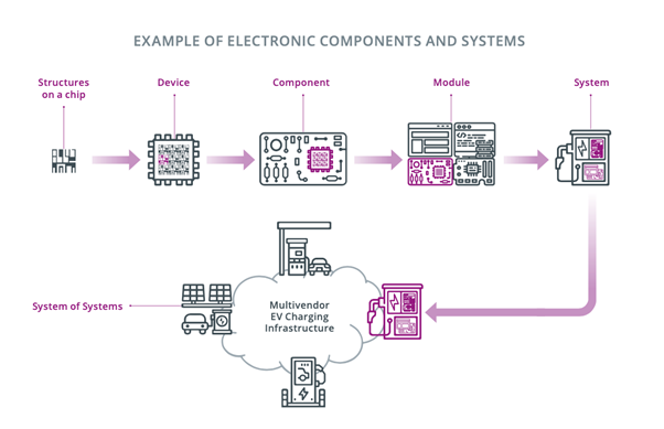
Designing such artefacts requires an interdisciplinary hierarchical approach, whereby various ECS specialists are working at different abstraction levels. As a result, the same term can have different meanings for specialists of different ECS domains: for instance, a “system” designed and implemented within a given development process may be integrated as a “component” into a higher-level “system” within another development step of the engineering process. Nevertheless, to avoid confusion, since 2021 the ECS SRIA includes a glossary, where many of the key terms are defined, to avoid inconsistency across the various chapters. It was also felt that developing a common language was important in building a strong and integrated ECS community. In addition, some of the bricks of the ECS technology “stack” are further detailed below.
- Device: in the context of the ECS SRIA, and if it is not further qualified, a device will be defined as a “packaged chip”, whether it is a packaged integrated circuit (e.g. system on a chip, memory, processor, or microcontroller) or a micro-electromechanical system (MEMS)/micro-opto-electro-mechanical system (MOEMS). A device performs a general electrical, electronic or electrical/electronic/physical transduction role.
- Component: a combination of devices and other elements (such as passives) that fulfil a specific need, such as transduction of a single physical parameter within a well-specified case. A component is not self-contained in all its functions, as it requires the close support of other components for operation (e.g. in data processing, power handling, and embedded software).
- Module: a combination of correctly integrated components in which their assembly embodies a specific functionality required for the proper working of a system (e.g. sensing and actuation module, control module, communication module, energy provision module). A module is self-contained in hardware and software, making it interchangeable between systems, and allowing a higher abstraction level in systems design.
- System: for the purpose of this SRIA, a system is a set of electronic-based constituents (subsystems, modules and components, realised in hardware, software, or both) that are integrated in a way that allows the system to perform a desired (set of) function(s). Due to ECS typically being constructed hierarchically, a “module” (e.g. camera or other sensor) being part of the electronic “system” in an autonomous car might itself be referred to as a “system” when being designed (e.g. while integrating lower-level components together to achieve the “camera” function).
- System-of-systems (SoS): a collection of independent and distributed embedded and cyber-physical systems dynamically composed to generate a new and more complex system, provided with new functionalities and driven by new goals not present in the constituent embedded and cyber-physical systems individually. The difference between a “system” (comprising subsystems, modules and components) and a “system-of-systems” (also comprising subsystems) is that the subsystems of a system are chosen and integrated during design-time (i.e. completely under the control of the engineers), while in a system-of-systems the constituent (sub)systems are physically independent and dynamically form a system-of-systems at run-time.
The first part of the ECS SRIA is composed of four chapters focused on the Foundational Technology Layers and their technical challenges along the technology stack, from materials and process technology to components, modules and their integration into electronic systems, embedded software developments and software technologies, to full systems and systems-of-systems. These foundational layers are characterised by hierarchical dependencies due to the inherent nature of ECS and the way they compose and integrate in complex structures. Advances in all Foundational Technology Layers will be essential to creating new electronic chips, components, modules, systems, and systems-of-systems along the value chain: these are the fundamental elements required to build the digitalisation solutions of the future.
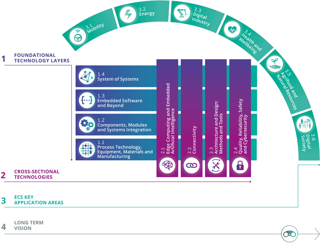
The foundational layers represent a very fertile ground where new interdisciplinary technologies, products and solutions can grow. They are then complemented in the second part of the ECS SRIA by four Cross-Sectional Technology chapters that focus on transversal areas of scientific research and engineering, where innovative results emerge from the joint contribution of the foundational layers to those specific areas. Edge Computing and Embedded Artificial Intelligence, or Connectivity (e.g. 5G to 6G) will require new integrated circuits to develop innovative electronic components that can be used to develop smarter and more connected components, modules and entire systems, running smart software that will offer new functionalities and capabilities. That will allow these systems to interact, cooperate and merge in larger systems-of-systems. Similarly, Architectures and Design: Methods and Tools have to be further developed to provide support to each of the foundational layers, covering all domains along the technology stack, across the entire lifecycle of technologies and products. The same applies to Quality, Reliability, Safety and Cybersecurity concepts that can only be addressed successfully if they are encompassing the whole ECS process flow along the entire value chain.
The innovation generated by these cross-sectional technologies will be applied across foundational layer stacks and amplify the effect of innovation in all key ECS application domains. Of course, there is some overlap among the eight technology chapters since they are closely linked, but as they examine the individual challenges from different perspectives, this overlap is extremely constructive and generates valuable synergies.
In the third part of the ECS SRIA, six Application chapters describe the challenges arising from specific ECS application domains that are key for Europe and identify the RD&I efforts required by these application domains as regards ECS.
Finally, the Long-Term Vision chapter illustrates our vision of the ECS beyond the time horizon covered by the other chapters. It seeks to identify the research subjects that must be addressed at low TRL levels as foundation and preparation for the crucial developments in European industry over the next decade. Based on the trends and plans described in the preceding chapters, the long-term industrial requirements are also examined to help research programmes understand which hardware, software and system solutions should be produced most effectively for the continuous improvement of European digital technology.
While the overall structure of the ECS SRIA is unchanged with respect to the previous edition, the internal chapter structure has undergone a significant revision: In particular, the sections “Strategic advantages for the EU” and “Technology-enabled societal benefits”, which were scattered across chapters in the previous edition, have been regrouped and summarised, to be now part of this introductory chapter. The rationale behind that restructuring is that many arguments developed in those sections were not chapter-specific but rather generic in nature. This allowed to avoid redundancies, refocus the messages of the individual chapters on their specificities, and reduce the overall ECS SRIA text size.
In the same spirit, the chapter editing teams have been reviewing their text with the goal to achieve greater conciseness, while of course eliminating outdated materials and providing new data.
Electronics components and systems are key digital technologies enabling the development of numerous applications. As such, the ECS research and innovation priorities are significantly driven by application roadmaps and needs. To that effect, the Key Application Areas part of the ECS SRIA translates application roadmaps into requirements for ECS. Conversely, the Foundational Technology Layers part maps out future advances and potential new breakthroughs in applications. The ECS SRIA therefore promotes synergies with many neighbouring application-oriented communities. For example, the Mobility Chapter (3.1) has strong links with ERTRAC; the Digital Industry Chapter (3.3) with EFFRA; and the Agrifood and Natural Resources Chapter (3.5) with the working group of the Alliance for the Internet of Things Innovation (AIOTI) in Smart Farming and Food Security, and with Water Europe16. In each case, experts participated in the work of both groups. There are also close interactions and alignments with European PPP initiatives, such as 2Zero and CCAM, IHI, etc.
The Cross-Sectional Technologies part also leverages the links of the ECS community with other technology-oriented domains, such as the European Technology Platform for High Performance Computing (ETP4HPC), EuroHPC, the European Working Group on High-Performance RISC-V based reference processing architectures, and Big Data Value Association (BDVA), with strong relations with the Edge Computing and Embedded Artificial Intelligence Chapter (2.1). Likewise, the Connectivity Chapter (2.2) benefited from fruitful exchanges with the 5G Infrastructure Association, SNS and inputs from the European Cyber Security Organisation (ECSO), as reflected in Chapter 2.4.
Several contributors of the Technology parts are also actively involved in the elaboration of international roadmaps (e.g. the Heterogeneous Integration Roadmap (HIR)17 in electronic packaging and integration, the IEEE International Roadmap for Devices and Systems (IRDS)18 for the semiconductor industry), and the RISC-V Roadmap of RISC-V International19 and the European Working Group20.
To summarise, this ECS SRIA combines application-pull and technology-push with the objective of enhancing the fertile dialogue between technologists and technology users, and strives to include discussions of upcoming strategic value chains.
Content wise, this revision was conducted with the goal to reflect the most recent technological and strategic trends of our industry. While already present in earlier editions, quantum technologies are getting additional attention in this new edition. The same holds for the irruption and disruption of AI tools in the practices of the ECS community, and the digital society at large. The importance of the RISC-V and Open-Source Hardware trend is further reiterated. Finally, the emergence of chiplets as a potential game-changer of our industry is discussed in this introduction, with several chapters going into the related technology requirements. The next pages provide some more details on the main changes of this edition.
Chiplets are not a package type, they are part of a packaging architecture. They are integrated circuit blocks that are specifically designed to communicate with other chiplets, to form larger, more complex ICs. Thus, in large and complex chip designs, the design is subdivided into functional circuit blocks, often reusable IP blocks, produced in suitable semiconductor material and process. These are called "chiplets", that are manufactured and recombined on high density interconnect, resulting in a shrinking of the PCB size.
Chiplets have some major advantages over SoC (System on Chip):
- Yield for each chiplet IP block is significantly higher +90% than for large SoC, 30-40%.
- A chiplet package becomes cheaper compared to a SoC.
- Time to market for chiplets are significantly shorter compared to SoCs.
- Modularisation allows for IP reuse
- Chiplets can be manufactured using the most adequate process technology in terms of cost, power and performance, while the monolithic SoC approach requires using the same technology for all IP blocks of the circuit
Current usage of chiplets is primarily in the high-performance computing server industry addressing AI applications. World leaders are NVIDIA, AMD, INTEL all supported by TSMC.
For the automotive industry, Tesla and some Japanese brands already use chiplets in their cars.
Chiplet technology has therefore the potential to lead to versatile and customizable modular chips, enabling reduced development timelines and costs. In addition, IP reuse improves design flexibility and efficiency. With all those promises, chiplets are sometimes touted as a revolutionary advancement in semiconductor technology2122. It is especially relevant for Europe, as a path to deliver innovative solutions while keeping the dependence relative to the dominant, non-EU advanced CMOS manufacturers to a minimum.
Chiplets manufacturing is addressed in Ch 1.2, while implications of chiplets are addressed in Ch 1.3, 1.4, 2.2 and 2.3.
Open-source hardware is hardware whose design is made publicly available so that anyone can study, modify, and further distribute the design, and/or freely make and sell hardware based on that design. The use of open-source hardware drastically lowers the barrier to design innovative SoCs. Indeed, this allows research centers and companies to focus their R&D effort on innovation, leveraging an ecosystem of pre-validated IP that can be freely assembled, modified, and customized for specific applications, whereas currently the cost of design of a set of IPs in-house is available to only few companies. And the use of alternative 3rd party IPs licensed by companies imposes constraints on innovation due to architecture. Open-source is also a sovereignty tool and avoids licensing IPs from foreign third parties, in a geopolitical context characterised by trade wars and export control restrictions.
While open-source SW approaches are now in wide use, open source HW has really drawn attention beyond the academic circles only in recent years. In China, USA and India, large governmental funded programmes have been created in order to stimulate the use of RISC-V and Open-Source in industry and products. The widespread adoption of this approach in Europe would have many benefits.
Creating an ecosystem to support open-source hardware is essential as it cultivates innovation and aids dissemination. This can be first based on the implementation of a strategic “Governance Initiative’’ to coordinate activities, maintain and promote the repository. Open-source projects only work well when they are attractive and provide innovation, but also when they are useful and trusted, so that at this point they can be self-supported by the community. One needs to make sure that knowledge is shared, accessible, maintained and supported on a long-term basis, as the success of open-source depends not only on the IP blocks but also on the documentation, support and maintenance provided. In particular, a one-stop-shop model with long-term activities and overall support (e.g., advice for licensing, productisation, etc.) can be promoted to help SMEs and start-ups.
The European strategy on open-source hardware should focus on application domains where there is a stronger impact, i.e. automotive, industrial automation, communications, health and aeronautics/defense. As these fields convey specific requirements (safety, security, reliability, power and communication efficiency…), the key differentiator between European core design efforts and existing players will be the attention given to the aforementioned requirements and also the extensibility with custom operations. Above all, a special focus should be placed on safety and security solutions, dealing with key aspects of collaboration, documentation, verification and certification in open-source communities.
A working group gathering European stakeholders was established in 2022. It drafted a technological roadmap starting with processors (RISC-V, beyond RISC-V, ultra-low power and high-end). The chiplet-based approach mentioned above is identified by the roadmap as a unique opportunity to leverage European technologies and foundries to create European HW accelerators interposers that could foster European More-than-More technology developments. Die-to-Die communication remains a missing link to leverage that approach, and its development in open-source is advocated by the working group.
In conclusion, the emergence of a European open-source hardware community should be encouraged and its initiatives be guided towards application domains where there is a strong impact. A technological roadmap has been drafted to build on the strengths of European industry and fill its gaps, while building blocks being developed will also need to be supported by the required tools, software supports, tests and documentation.
Disruptive technologies, where market positions are not established yet, are level-playing fields where Europe has all its chances to gain leadership. Quantum technologies fall in that category and therefore their evolution and maturity are closely monitored by the ECS SRIA expert community. The importance of the technologies is identified in both the Chips Act and in the European Quantum strategy23. Together with the European Quantum Flagship SRIA, these documents highlight areas of importance and overlap with the ECS SRIA:
- Technologies for dedicated quantum chips, required to fulfil the quantum challenges.
- Classical chips technologies for quantum (enabling technologies) required to support the industrialization and scaling of quantum technology.
- Systems combining these two for applications taking advantage of quantum technology.
Quantum technologies are very diverse in nature, encompassing quantum computing and simulation, quantum communication, and quantum sensing and metrology24. As application fields, they go beyond the scope of the ECS SRIA, but the community should prepare for using quantum technology in the applications that can benefit from quantum chip technologies, e.g. in navigation and timing using quantum sensors.
Quantum chip technologies include six major modalities: Superconducting circuits, semiconducting quantum dots, ion traps, photonics, neutral atoms and nitrogen vacancies in diamonds. All of these technologies have their specific chip technology development needs. The technologies combine traditional microfabrication technologies in Silicon and other substrates with novel primitives that use quantum physics on single electron/atom/ wavefunction level, with RF and optical control and readout. As an example, ion trap quantum systems combine RF electrodes for ion trapping for with optical control of trapped ions.
Quantum technologies use have special material needs, such as the use of isotopically pure Si, and specific processing needs, such as Al/AlOx/Al tunnel junctions with extreme requirements for dielectric tunnel barrier quality and thickness control. In integrated photonics, the needs of the quantum systems typically include extremely low losses and wavelengths in the visible range, from 800-900 nm as low as 300-400 nm, depending on the atoms or ions used.
In applications, quantum computing is projected to have the largest market size and impact to many application fields. Estimates vary, but quantum computing market growth to 28 B€ in year 2035, with full value chain, including application benefits, potential to be over 1 trillion Euros25. However, quantum sensors while being a smaller market, may be considered more mature, with sensors already use in application, such as: superconducting SQUID magnetometers in biomagnetism and brain imaging diagnostic sensors or quantum sensors in GPS free navigation.
In particular, the emerging field of quantum computing poses its own challenges for the ECS community in process technology, equipment, and materials:
- As there are still several candidates for becoming the standard quantum computing technology, a wide range of materials is relevant, together with innovations in process technology.
- New metrology capabilities are required, especially the measurement of electrical properties, such as local carrier mobility.
- To achieve practical applications, reliable fabrication, connection, and read-out of qubits need to be developed.
- The low temperatures, from milliKelvins to 4 K, at which many quantum systems are operated requires the development of cryogenic devices, to interface conventional electronics.
Beyond quantum computing, all quantum technologies related to sensing, communications and computing, including software, present significant challenges today relevant for the ECS SRIA. Given the level of maturity of those technologies, especially when it comes to quantum computing, those challenges are mainly discussed in the Long-Term Vision chapter, but research focus areas derived from the needs of quantum technologies can also be found in other chapters of this document. This reflects that quantum technologies maturity is expected to evolve rapidly in the years to come, and that Europe should leverage its assets, with excellent research centres and a dynamic ecosystem of start-ups, to gain leadership in that promising field.
Similarly to quantum technologies, spintronics (excluding MRAMs which are already at a commercial stage) belongs to the category of disruptive technologies, where market positions are not established yet and Europe has the opportunity to gain leadership. This is an emerging field that holds significant potential to become a key component of future energy efficient chips technologies. The high performance and ultra-low power consumption intrinsic of such technology, make it a very attractive solution to the increasing demands for computing power, notably with the growing market of AI. By combining processing, logic, sensing and storage on a unified platform, spintronic devices can advance technologies such as neuromorphic electronics, unconventional and quantum computing, and energy harvesting, significantly contributing to low-carbon footprint prospects. Europe is well positioned with world-leading institutes in the domain
With the development of the global internet traffic, AI/ML and IoT, the demand for data centers and high-performance computing (HPC) is increasing. An extremely large link capacity for high-speed datacom interconnects between multi-cores or local/distant caches becomes compulsory. However, it is becoming increasingly difficult for the conventional electrical Cu interconnects to meet such an ever-growing capacity requirement since they severely suffer from limited bandwidth, significant power consumption, integration difficulty on racks and material cost and mass.
Silicon Photonic Integrated Circuits (PIC), referred to as Si-photonics, is the technology that realizes photonic components and circuits on Si substrates using materials and fabrication process flows in the well-established microelectronic industry. Replacing electrons with photons to transmit data brings advantages including high-speed operation, low power consumption and high-capacity transmission. Building photonic integrated circuits (PICs) based on industry-standard Si platform promises additional merits, namely lower cost, high-volume manufacturing, large integration density, advanced functionality and high scalability.
Furthermore, Si-photonics, with their CMOS compatibility and small size, weight, area, and power consumption, have the capability of accommodating growing volumes of computer data arriving in real time and at very high rates in large-scale distributed computing systems. The wavelength and spatial multiplexing properties of optics are beneficially translatable to executing critical bandwidth and communications-intensive connections between increasingly parallel computational resources.
Benefiting from an ideal Si/SiO2 interface and a large refractive index contrast, Si is an ideal platform for implementing passive optical devices such as low-loss waveguides, mode converters, and multiplexers/demultiplexers. Although Si is a centrosymmetric crystal and, thus, not an ideal material for optical modulators, high-performance modulators have been demonstrated. Efficient Ge- and SiGe-based photodetectors operating in the telecom bands are also selectively grown on Si-photonics wafers.
However, if Si can efficiently transmit, modulate, and detect light, its indirect band structure precludes efficient light emission. The achievement of on-chip light sources, using Ge alloys for instance, represents a significant challenge in advancing the complete integration of silicon-based PICs. Therefore, III-V material (InP, GaAs) on-chip lasers are currently embedded in PICs using 2.5 and 3D heterogeneous integration. Monolithic integration of III-V materials is an attractive alternative due to its high integration density. However, it introduces a high density of crystalline defects, significantly degrading the laser’s performance. Exploring methods of reducing these defects is paramount to advance monolithic integration toward high-density, large-scale silicon-photonic integration.
Similarly, for applications that require high-speed modulation, the properties of Si-based modulators are not sufficient. Hence, ferroelectric electro-optic materials such as, III-V semiconductors, LiNbO3 and BaTiO3 should be embedded in the PIC using heterogeneous integration (die-to-die, die-to-wafer, or wafer-to-wafer bonding). Also, improving the quality and performance of waveguides, passive and active photonics devices sometimes requires the introduction other dielectric materials such as nitrides.
The most established form of the technology is optimized for operation in the telecommunication wavelength bands near 1310 and 1550nm and has waveguides defined in the top Si device layer of a silicon-on-insulator (SOI) wafer. It is enabling power-efficient transceivers and large-scale PICs that address the demands of data communications. Three-dimensional (3D) sensing, and computation accelerators are other applications for which convincing demonstration exists. In addition to these applications, there is a growing demand to develop silicon-photonic for new product applications that include chip-to-chip electrical/optical interconnect, automotive LiDAR (in particular for beam steering without any moving part), quantum computing, infrared imaging and biomedical and environmental sensing. The last three applications require the development of PICs in the mid-IR region wavelength range (2–20μm) as it contains strong absorption signatures of many molecules, which requires different sets of materials.
While not a totally new topic (it is used for example in several embedded systems for vision, enabling autonomous vehicles), artificial intelligence (AI) really came to the forefront for the public at large in 2023, with tools such as Chat-GPT (released for public use only on November 30th, 2022) and other generative AI (Dall-E, Stable Diffusion) that grabbed the headlines in mainstream media. The ECS Research and Innovation roadmap interacts with the development of AI tools and algorithms in two symmetrical ways: ECS are an enabler for new AI developments, and AI can in turn be a significant enabler for new ECS advances. Those two aspects are extensively discussed in this current edition of the SRIA.
- ECS as enabler of AI: Chapters 1.1 and 2.1, as well as the Long-Term Vision Chapter, stress the importance of moving the processing of AI algorithms locally on a hardware device (in deep-edge devices, edge devices or on-premise computing resources, depending on the application) close to where the data is generated (e.g. by a sensor), a trend known as “embedded AI” or “edge AI”. Benefits include reducing the energy consumption of the data infrastructure by transmitting only relevant data or pre-treated information, improving data protection, increasing security and resilience due to a reduced reliance on telecommunication links, reducing latency, and decreasing memory footprint. Many of the focus research areas identified in Major Challenge 1 (Advanced computing, in-memory, neuromorphic, photonic and quantum computing concepts) of Chapter 1.1 support this move towards AI at the edge. Likewise, the four Major Challenges (increasing energy efficiency, managing system complexity, increasing device lifespan and ensuring European sustainability of embedded intelligence), identified by Chapter 2.1, all cover research topics which will enable the development of a strong European embedded AI ecosystem. Energy consumption of AI solutions is an overarching issue due to the expected widespread increase of their usage, and it is essential to explore new concepts and architectures (bio-inspired and other ones) to respond to that concern, which could turn out to be a major roadblock if not addressed properly.
- AI as enabler of ECS: this aspect is discussed in Chapter 2.3, where several examples of AI use are listed to tackle Major Challenge 3 (managing complexity), such as AI-based methods for the architecture exploration and optimisation, to achieve a global optimum, AI-based guidance in the V&V process, and automatic generation of test cases with AI support. Moreover, in its entirely new section devoted to Machine Learning and Artificial Intelligence, the Long-Term Vision Chapter states that AI/ML methods are increasingly adopted in design space exploration at several stages of circuit design, as well as in design testing and verification. The potential of these AI-based methods is not limited to circuit design and extend to large-scale ECS products encompassing HW and SW, as well as multi-physical, distributed systems. They are also expected to provide guidance to engineers in multi-risk (safety, security, privacy, and other trustworthiness risks) optimisation problems. Gathering / generating the appropriate data to train the models is identified as one of the most difficult issues to be addressed.
A third aspect is that AI adds complexity to the systems it empowers. This in turn raises additional issues at the design phase, as addressed by Chapter 2.3. There, Major Challenge 1 (Enabling cost- and effort-efficient Design and Validation Frameworks for High Quality ECS) stresses the need to develop new design and verification and validation methods for AI-based ECS, including ECS evolving during lifetime.
Finally, a purely technical approach to develop trustworthy and explainable AI, or having AI in the loop with verification of its results might not be enough to address the growing public concerns about the potential dangers of AI (pushing many governments across the world to sign the Bletchley Declaration on AI safety). In the years to come, cooperation between multidisciplinary partners with backgrounds in AI, ECS and social sciences, as well as access to “foundation models” by European academia and industry will be required to achieve and ensure the acceptance of efficient and responsible AI-based ECS, reflecting European values.
The energy world is undergoing a radical transformation, dominated by three factors: installation of renewable energy sources, transition to carbon neutral mobility and massive growing demand for AI datacenters. Promoted by EU and national roadmaps, the globally installed capacity of renewable generation has doubled within the past 10 years. Europe alone expanded its renewable generation capacity by 10% in 202326. This increase is dominated by wind and solar energy being characterised by strongly intermittent, distributed generation. The share of wind and solar of Europe's electricity generation reached a record high of 26.6% (718 TWh) in 2023, almost twice the global share of 13.4%.
Highly efficient, reliable, affordable power electronics and power system control are the core elements from the ECS side contributing to the transition. Lower costs are key to safeguard the tremendous societal change, since current high energy prices are one essential factor leading to instabilities and are a thread towards the change to a carbon neutral society.
Having on one side the energy transition challenge, electricity generation from renewables, heating towards heat pumps, mobility towards electric mobility the next challenge is evident – the energy consumption of the AI data centers. According to a study by McKinsey27, global demand for data center capacity could rise from the demand of 60 GW in 2023 at an annual rate of between 19 and 22 percent until 2030 to reach an annual demand of 171 to 219 GW.
The need is given with the upcoming AI capabilities – the challenge is to reduce the energy demand by algorithms and more and more efficient power supply – closer and closer to processor units, more and more efficient. This huge market, driven by the three factors energy system transition, mobility and data centers, is attractive, hence globally research and expansion of fab capacities for power electronics is booming. To keep the technology competence, to serve the demand from European based manufacturing research and investment in Europe is mandatory in the fields of the core technology serving the electricity demand of the future.
Device architecture, the excellence in achieving extremely thin wafer thicknesses, and for the wide bandgap technologies the move to larger wafer diameters are core technology capabilities in Europe which should be further strengthened to keep a significant manufacturing and knowledge share in Europe. Vision is to serve the energy transition with highest efficient, reliable, sustainable manufactured power electronics and be capable to have the system competence to design beyond state-of-the-art power systems, for the renewables, electric mobility and for the powering of the AI data centers.
On top of these general trends, individual chapters also reflect the latest evolutions:
In Chapter 1.1, Process Technology, Equipment, Materials & Manufacturing, application breakthroughs are now classified by sector, extending to new domains such as AI & Energy, Defence and Space, and Flexible Electronics. The chapter also introduces material-related challenges that complement several existing Major Challenges.
In chapter 1.2, Components, Modules and Systems Integration, the topics “Advanced integration solutions” and “Heterogeneous integration” have been merged into a combined major challenge “Advanced & Heterogeneous integration”.
Chapter 1.3, Embedded Software and Beyond introduces a new Major Challenge on embedding agentic AI in software systems, alongside expanded consideration of AI in software development. Resilience and Dependability aspects have been added to Major Challenge 6 (Software reliability and trust), while Major Challenge 4 (Embedding data analytics and AI) now includes Embedded AI. The chapter also broadens its coverage of Open Source, including its use in safety-relevant applications.
In Chapter 1.4, System of Systems, the engineering and management of SoS are now discussed in the context of the introduction of chiplets and the creation of an edge-to-cloud compute continuum, underlining the architectural impact of these trends.
The chapter 2.1 foregrounds Generative/agentic AI at the micro- and deep-edge, with stronger emphasis on energy-proportional, privacy-preserving on-device compute and aggressive quantization, while adding beyond-CMOS and neuromorphic/in-/near-memory approaches within an edge-to-cloud continuum.
Regarding Cross Sectional chapters, Chapter 2.2, Connectivity, has been updated to address the introduction of chiplets and its impact on both hardware and software.
Chapter 2.3 pivots toward AI-enabled, virtualised engineering across the lifecycle—emphasising MBSE with VP-ready models integrated into CI/CD, Digital-Twin–based validation, and value-chain “Digital Threads,” with updated scope references to SDV and edge/cloud architectures.
Chapter 3.1 emphasizes more Software-Defined Vehicles and edge-to-cloud applications, adding a RISC-V automotive hardware-platform roadmap. It introduces a two-speed delivery model, strengthens OTA-driven lifecycle management with digital twins and CI/CT/CD and adds Cloud-Edge-IoT service use-cases and RDI topics such as V2X and bidirectional charging.
Within the Application chapters, Chapter 3.2, Energy, has been brought up to date with new data, figures, and references, and aligned with recent changes in the European Union’s energy strategy.
Chapter 3.3, Digital Industry, expands its coverage of Generative AI with concrete industrial use cases, introduces an updated EU framing via the 2025 AI Continent Action Plan, and adds guidance on reliable data acquisition using software/virtual sensors across operating conditions. It also newly emphasises Edge AI in robotics for manufacturing and automation.
Chapter 3.4, Health & Wellbeing, extends its discussion of AI-related topics, explicitly addressing staff shortages in healthcare, while reinforcing the focus on privacy-by-design, data trust, AI ethics, and sustainability.
Chapter 3.5, Agrifood & Natural Resources, introduces new detail on Geospatial AI (GeoAI) for precision agriculture, quantum sensors and advanced photonics for environmental monitoring, cybersecurity and data privacy in agricultural ECS, real-time edge computing architectures for remote applications, interoperability standards, and wearable technologies to support human operators.
Finally, Chapter 3.6, Digital Society, has been revised to reflect the continued evolution of AI-based tools. In addition, an added motivation underscores the need for affordable ECS solutions, connecting this to broader societal tensions arising from demographic, economic, climatic, and digital technology pressures in Europe.
The 2026 ECS SRIA lists a number of milestones to be reached in the short term (2026–2030), medium term (2031–2035) and long term (2036 and beyond) via collaborative research projects across Europe, reflecting the ambition of the ECS industry towards the achievement of the five Main Objectives identified above.
The following figures summarise the most salient milestones to be reached in the various domains covered by the ECS SRIA over the three time periods:
- Short term (2026–2030)
The industry has a precise idea of what will be achieved during this short-term timeframe.
- Medium term (2031–2035)
There is already reasonably good knowledge of what can possibly be achieved.
- Long term (2036 and beyond)
Expected achievements are more of a prospective nature.
Including a milestone in each of these time periods means that the described features are expected to be available at TRL levels 8–9 (prototype or early commercialisation) within that timeframe. For example, the Components, Modules and Systems Integration Chapter expects that, within the next five years (short term), the materials that enable recycling and repair will be available. These materials will allow for the deployment of the monitoring of forests, fields and oceans, as envisioned by the Agrifood and Natural Resources Chapter over the same time horizon. In parallel, this monitoring will gain in efficiency due to the development of advanced AI edge solutions leveraging open source or alternative strategies, as forecast by the Chapter on Edge Computing and Embedded Artificial Intelligence.
The above example also clearly shows that progresses in the various domains covered by the ECS SRIA are deeply interconnected. Innovation in one area is building upon, or being driven by, innovation in other areas. Similar examples could, of course, be developed for the other time horizons, as represented in Figure 0.6, 0.7 and 0.8. More detailed diagrams, including additional milestones, are presented in the individual chapters.
The following tables show the updated timeline items for 2026, followed by the original diagrams from the 2025 version. The updated information from some chapters is still missing at this point, but details may be found in the respective chapters.
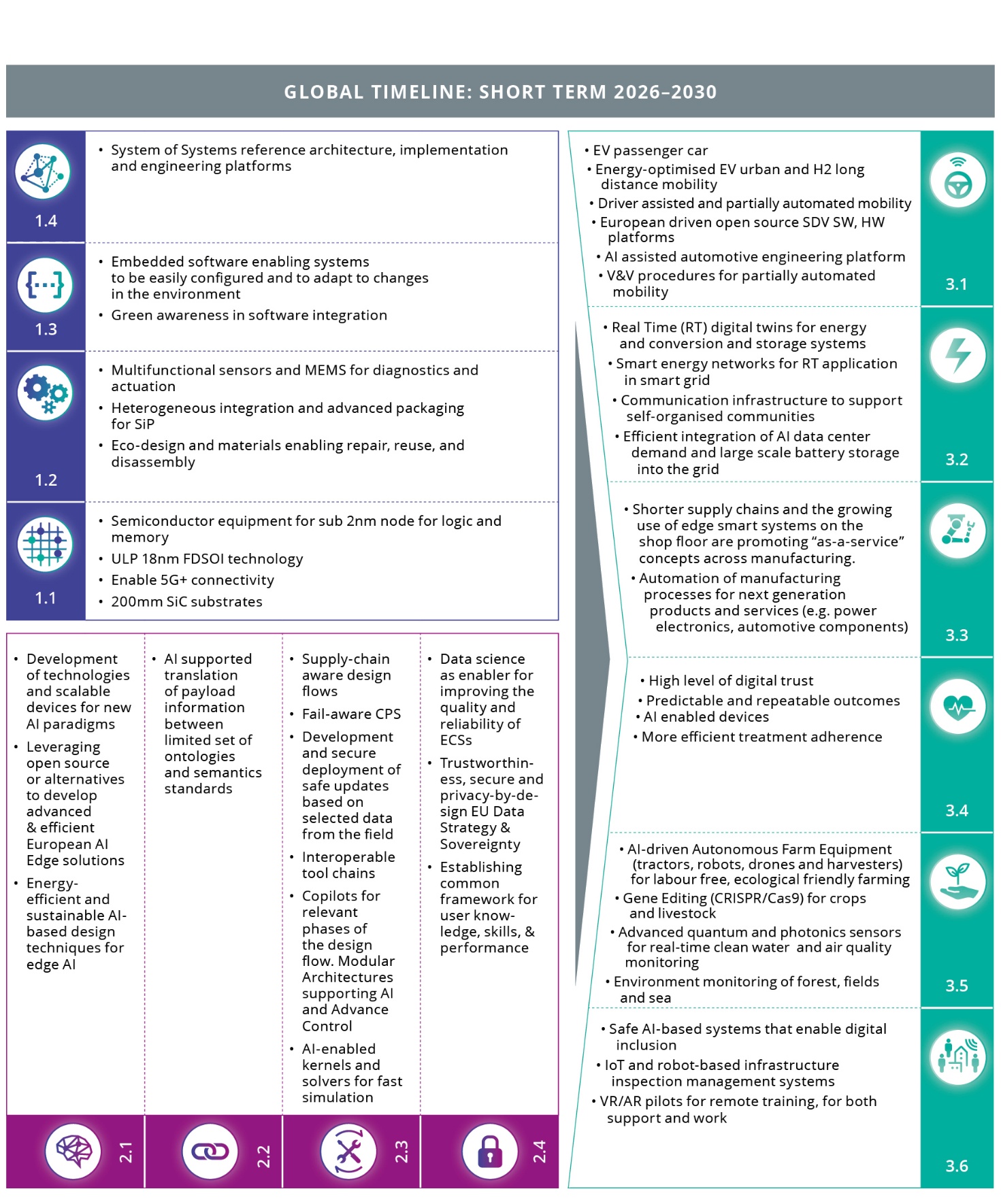
Figure 0.6 Global Timeline: Short term 2026–2030, for comparison
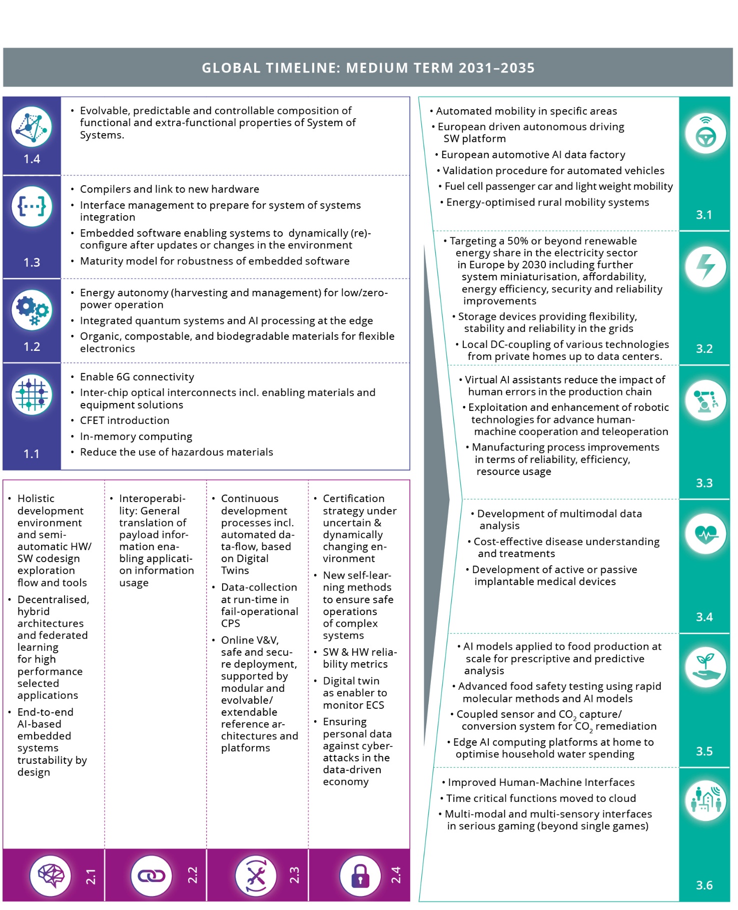
Figure 0.7 Global Timeline: Medium term 2030–2034, for comparison
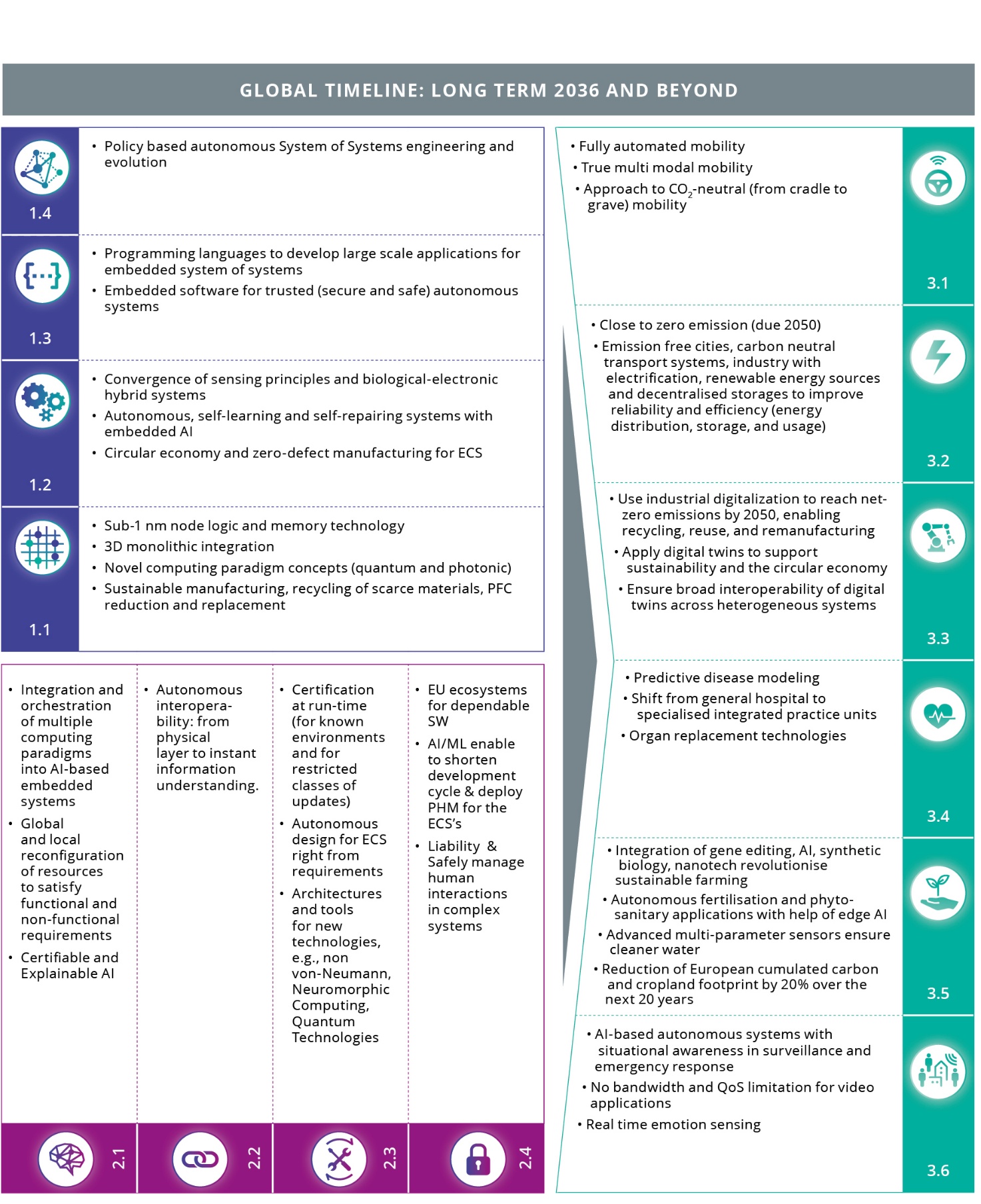
The following diagram provides an outline of the entire ECS SRIA to clarify the roles of the chapters, the technology domains they cover and the synergies between them, simplifying the comprehension of the ECS SRIA and its “navigation”.

Figure 0.9 SRIA outline
As mentioned, the ECS covered by this document is very wide-ranging, and involves many technical disciplines in materials, processes, hardware and software. Therefore, most readers will only want to read those chapters that cover the disciplines of their interest, without being willing to go through all the technical details presented in the ECS SRIA.
For each technology and application domain it covers, the ECS SRIA identifies specific so-called Major Challenges, with a focus on the most critical aspects to be tackled from the perspective of innovation. The analysis of each Major Challenge illustrates the state of the art of the associated technology and/or application domains, describes the vision of the ECS community for the future, identifies potential outcomes, and defines research and engineering activities on the key focus areas that are fundamental to successfully address the challenge.
The structure of all the Foundational Technology and Cross-Sectional chapters is identical. In the Key Application Areas chapters, the authors explore each domain with the application demands as the main focus, not the technical challenges.
A Glossary describing the terms used in the document, as well as a List of Acronyms used in the document, can be found in the Appendix. The Analytical Index available in earlier releases of the ECS SRIA is now substituted by an advanced Search functionality. At the end, the reader can also find a List of Contributors who collectively wrote this ECS SRIA.
Finally, to highlight the synergies/links between the chapters and provide hints to the reader, cross-references have been introduced alongside the text.
Cross-references consist of the Chapter icon and appear alongside the text. When hovered on, they indicate the relevant chapter number and the topic or concept described in the text is also highlighted. When clicked on, they will navigate you to the referenced Chapter.

References within a text are indicated by small numerical markers embedded in the content, e.g. Upon clicking one of these markers, readers are instantly directed to the corresponding entry within the References section. This feature allows readers to seamlessly access the sources from which the information has been derived.
Furthermore, by clicking on the same footnote number located in the References section, readers can effortlessly return to the exact point within the main text where the reference was initially cited. This interactive function not only enhances the reader's comprehension but also streamlines the process of verifying and exploring the sources behind the presented information.
- https://ec.europa.eu/digital-single-market/en/policies/building-european-data-economy↩︎
- https://eur-lex.europa.eu/legal-content/en/TXT/?uri=CELEX:52021DC0118↩︎
- Europe’s urgent need to invest in a leading-edge semiconductor ecosystem - Article - Kearney↩︎
- European Parliament: EVP Dombrovskis speech at hearing Commissioner-Designate for Trade https://ec.europa.eu/commission/commissioners/2019-2024/dombrovskis/announcements/european-parliament-evp-dombrovskis-speech-hearing-commissioner-designate-trade_en↩︎
- Source: Embedded Intelligence: Trends and Challenges, A Study by Advancy, Commissioned by ARTEMIS Industry Association, March 2019↩︎
- A collection of independent and distributed embedded and cyber-physical systems dynamically composed to generate a new and more complex system, provided with new functionalities and driven by new goals not present in the constituent embedded and cyber-physical systems individually. See full definition in the glossary↩︎
- From Internet of Things to System of Systems – Market analysis, achievements, positioning and future vision of the ECS community on IoT and SoS, P. Azzoni, Artemis 2020.↩︎
- An integration platform is an ECS allowing the integration of different systems, applications and services into a single system. See full definition in the glossary↩︎
- Semicon Coalition calls for reinforced Chips Act | Shaping Europe’s digital future↩︎
- The Draghi report on EU competitiveness↩︎
- Europe’s Digital Decade: digital targets for 2030 | European Commission (europa.eu)↩︎
- Pact for Skills - Employment, Social Affairs & Inclusion - European Commission (europa.eu) Pact for Skills - Employment, Social Affairs & Inclusion - European Commission (europa.eu)↩︎
- More than 81% of produced software are consuming open-source code in products or services (https://github.com/todogroup/osposurvey/tree/main/2020)↩︎
- PFAS is a class of thousands of synthetic substances known as ‘forever chemicals’ since they do not break down in the environment. PFAS offer a unique set of technical characteristics, which include exceptional heat and chemical resistance, high electrical insulation resistance, high purity, low-outgassing and low coefficient of friction↩︎
- Structure on a chip: elementary building blocks of an integrated circuit, such as a FDSOI or FinFET transistor, or more complex structures such as an embedded memory block.↩︎
- https://watereurope.eu/wp-content/ uploads/2019/07/Water-Europe-SIRA.pdf↩︎
- https://eps.ieee.org/technology/ heterogeneous-integration-roadmap/2019- edition.html↩︎
- https://irds.ieee.org/↩︎
- RISC-V-Introduction-_-Aug-2021.pptx (live.com)↩︎
- https://digital-strategy.ec.europa.eu/en/library/recommendations-and-roadmap-european-sovereignty-open-source-hardware-software-and-risc-v↩︎
- John Lau, Chiplet Design and Heterogeneous Integration Packaging, Springer 2024↩︎
- Cadence PCB solutions, https://resources.pcb.cadence.com/blog/2023-all-about-chiplet-technology, consulted 25 July 2024↩︎
- Quantum Europe Strategy: Quantum Europe in a Changing World, COM(2025) 363 final, European Commission↩︎
- Strategy Research and Industry Agenda, Published in February 2024 by the European Quantum Flagship↩︎
- McKinsey & Company: Quantum Technology Monitor 2025↩︎
- https://www.irena.org/-/media/Files/IRENA/Agency/Publication/2024/Mar/IRENA_RE_Capacity_Statistics_2024.pdf↩︎
- https://www.mckinsey.com/industries/technology-media-and-telecommunications/our-insights/ai-power-expanding-data-center-capacity-to-meet-growing-demand↩︎