
1 Foundational Technology Layers
1.2
Components, Modules and Systems Integration
Development and production of smart electronic components and systems (ECS) requires physical and functional integration (PFI) of several functionalities into a new physical entity at component, module and system levels (CMS). Therefore, PFI is one of the essential capabilities required to maintain and improve the competitiveness of European industry in the application domains of smart systems. Although in practice PFI is often application-specific, the materials, technologies, and manufacturing processes that sustain these domains are generic and should be standardized, interoperable and reconfigurable whenever possible.
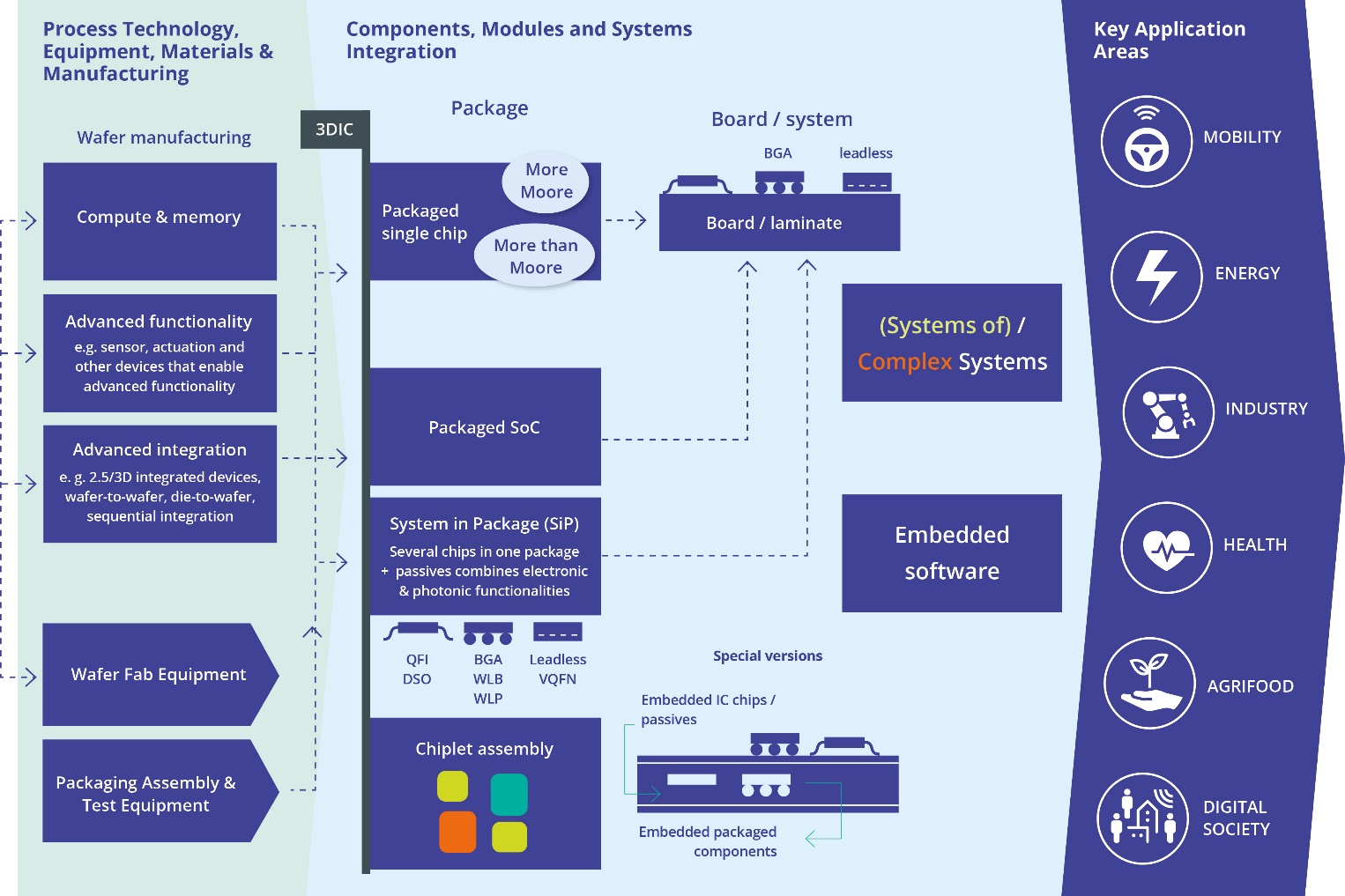
As smart systems and innovative products continue to evolve, heterogeneous integration is becoming increasingly important at all levels—from semiconductor Systems-on-Chip (SoC) to Systems-in-Package (SiP), and up to larger modules and complete systems. The significance of SiP technologies in this integration process is highlighted by their coverage in both this chapter and Chapter 1.1, each offering a different perspective. While Chapter 1.1 focuses on semiconductor technologies, material families, and on-chip systems (SoC), this chapter explores integration approaches beyond that scope. It places particular emphasis on alternative technologies (e.g., additive manufacturing), complementary materials (both functional and structural), and heterogeneous methods for assembly, integration, and advanced packaging.
The term heterogeneous integration is used in its widest meaning: a component should be taken to mean any unit, whether individual chiplet/die, MEMS device, passive or active component or assembled package, that is integrated into higher order single components, modules or systems. Developments of heterogeneous integration technologies and platforms include also flexible electronics and photonics solutions. On the other hand, advanced packaging represents the suite of novel technologies, processes and competences that – in a cost-efficient, environmental sound way – allows for the physical, electrical and functional integration of any set of technological diverse components required to build an advanced system in a way that can safely interact with its application environment.
Smart CMS technologies serve as the crucial link between foundational technologies—such as semiconductors and interconnection—and the key applications outlined in the Application Chapters. By integrating functions like intelligence, sensing, communication, and control—even into the smallest devices—they enable broad adoption across all application domains. This is achieved through the simultaneous development and co-design with Embedded Software and System-of-Systems (SoS) technologies, supported by cross-cutting technologies including Artificial Intelligence (AI), Connectivity, Architecture and Design, and Quality, Reliability, Safety, and Cybersecurity.
The methods, processes and schemes required for the design, production, assembly and testing of the various CMS and their integration need to be devised with appropriate quality, reliability, repeatability as well as scalability and sustainability (circular economy, CO2 footprint, life cycle considerations, efficient use of resources).
Given the evolving demands of current and future smart systems, the ability to master integration technologies at the different CMS levels is a key strength of European industries. Maintaining and strengthening this capability is essential for Europe to retain its leadership in smart systems engineering and to translate innovation into reliable, sustainable products, services, and markets.
Future smart CMS will feature a strong increase in functional and structural complexity and higher integration levels. They will show more diverse features and material integration in even smaller form factors. Technology advances at CMS level will have a key impact on applications of all sorts.
As society continues to undergo widespread and consistent digitization across all sectors—including edge-IoT applications, mobility, telecommunications, and healthcare—certain technological requirements are becoming increasingly critical. These include cyber-resilient and long-term digital storage of data, operating systems, firmware, and boot media; extended operational lifetimes; and adaptability to changing conditions, whether for everyday use or critical applications and infrastructure.
Applications are the drivers for such approaches:
- Communication landscape with 5G, 6G and increasing data rates, including non-terrestrial networks (NTN), time-sensitive networks (TSN) as well as navigation and localization, including optical integration, components and systems for fiber networks.
- Autonomous systems in mobility, transport, logistics, manufacturing or control of buildings and micro-grids, etc., ensuring faster time response and decreasing the impact of human error.
- Monitoring at remote or difficult to access locations, e.g., structural health monitoring of infrastructure (bridges, tunnels, civil structures) or harsh environments supported by unattended systems, able to operate reliably with power autonomy and decision-making enabled at the edge.
- Healthcare landscape with applications moving towards prevention, diagnostics, therapy and rehabilitation, and life science and pharma domains is moving towards both personalized medicine and regenerative medicine smart multifunctional systems, deployable in the body, on the body or around the body.
- The transition in mobility towards zero-emission power trains, with their significant cost and energy efficiency challenges, including energy systems for high-power charging and/or highly variable and changing conditions.
- Industry 4.0 manufacturing landscape to enable agility and autonomy, as well as energy and resource efficiency, including manufacturing down to lot-size-1.
- Progression to scalable, fault tolerant and ultimately self-monitoring and repairable/re-configurable networks particularly for long life span applications such as environmental and structural health monitoring.
- Sensing of environmental parameters in smart agriculture, livestock or aquaculture, in manufacturing and working places, at home and in urban areas, e.g. for higher yield, energy efficiency and well-being.
- Imaging and audio applications—including VR, MR, and AR— increasingly used in sectors such as security, healthcare, digital industry, precision agriculture, food production, and the digital society (e.g., television and social media). These applications demand electronic, spintronic, photonic, and information systems that are deployable, portable, and highly functional.
- Space applications, including satellite communications, Earth observation, and autonomous deep-space missions, requiring state-of-the-art electronic and photonics systems and advanced packaging solutions for ultra-reliable, miniaturized, and radiation-hardened operation.
- Dual-use, security and defence applications for example in communication, computing, surveillance, sensing, imaging and signal intelligence. These have a growing importance not just for the military defence applications but also for civil security in protecting critical infrastructure and countering cyber and hybrid threats.
- Enabling repair as business, including repair index and set-up of repair processes. This also includes self-monitoring for condition evaluation.
The following Major Challenges are identified:
- Major Challenge 1: Functionality. Developing new features for power, sensors, actuators and smart systems via new materials and methods enabling miniaturization and optimized performance.
- Major Challenge 2: Advanced & Heterogeneous Integration. Development and deployment of leading-edge packaging and heterogeneous integration technologies that combine advanced materials, design methodologies, metrology, inspection and testing approaches, and chiplet/system-level integration, emphasizing cost-effective system–technology co-optimization.
- Major Challenge 3: Sustainability. Sustainable components, modules and systems and their integration processes to minimize their environmental impact over the entire lifecycle.
1.2.3.1 Major Challenge 1: Functionality
Physical and functional integration (PFI) considers the development of new elements and methods enabling more functionalities to be physically integrated on CMS in the most effective form factor. This requires interdisciplinary technology innovations as smart CMS may utilize a combination of features based on nano-electronics, micro-electro-mechanic, thermoelectric, magnetic, photonic, micro-fluidic, optical, acoustic, radiation, radio frequency, biological, chemical and quantum principles. Furthermore, many types of devices are to be integrated together, such as sensors, actuators, energy generators, energy storage devices, data processing devices, transceivers and antennae. Different technological approaches such as mainstream silicon technologies, MEMS/NEMS, MOEMS and LAE (Large Area Electronics) can be combined for the synergistic assembly of electronic and photonic devices.
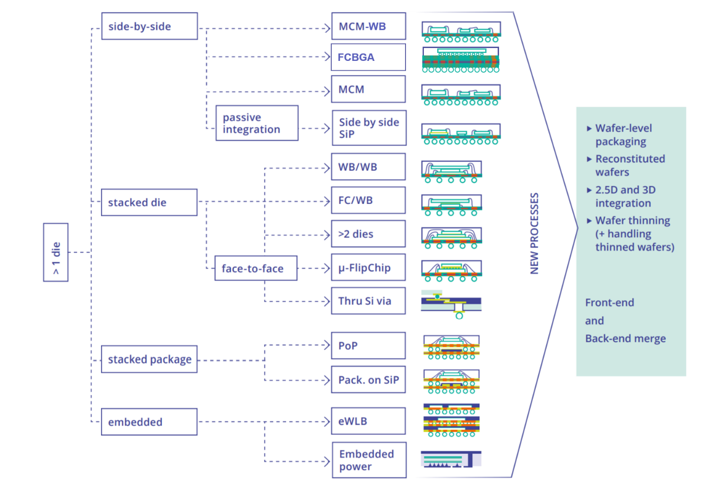
PFI goes beyond the compact monolithic SoC approaches supported by the semiconductor technologies covered in the Process Technology, Equipment, Materials and Manufacturing Chapter. It addresses System in Package (SiP) realizations involving different integration methods of components with a higher degree of technological heterogeneity into different platforms, including Integrated Circuit carriers, PCB boards, additive manufacturing on flexible or hybrid substrates, and co-packaging of optics and electronics.
PFI requires not only the integration of physical components together, but also the co-design and integration of software, especially embedded software and embedded AI accelerators, to create reliable and sustainable functional systems. This also extends to the development of modular architectures that enable such systems to be configured dynamically and optimally for a given application. However, this chapter concentrates on the physical integration of hardware, including computational devices into systems, while leaving the software edge to the Embedded Software Chapter.
Given the broad range of physical scenarios they face, smart CMS need to interact with many environments, once outside the lab, including demanding ones such as harsh environments or in-vivo.
CMS face numerous operational challenges related to energy, performance, and size. In terms of energy, portable IoT devices require ultra-low-power operation and some form of energy autonomy—either through self-powering or by providing sufficient autonomy to meet specific application requirements (e.g., lifetime, service intervals). At the same time, for power electronics applications, they must address issues of high current density and the resulting thermal stress. For size, achieving the optimal minimum footprint at a given application is critical. This calls for the use of heterogeneous integration alongside advanced packaging and interconnection technologies to deliver maximum performance in the smallest possible system-level form factor, with minimal power consumption—or at least with consideration of available energy resources. In high-end consumer electronics, high-performance, ultra-dense, and compact interfaces across all integration levels—from chiplets and chip assembly/packaging to component and module connectors – shall be met. Increasingly, these systems may also incorporate photonics-based communication to meet data transfer and efficiency needs.
The development of MEMS/NEMS/MOEMS technologies centers on sensors and actuators that exploit the free surfaces and volumes achievable through semiconductor-based microfabrication. Sensors include next-generation inertial measurement units (accelerometers and gyroscopes) with enhanced performance—optionally augmented by AI—alongside magnetometers, pressure sensors, microphones, and particle sensors. The integration of advanced spintronic sensors, particularly those based on TMR technology, will further enhance these capabilities by providing ultra-sensitive, low-power magnetic field detection suitable for edge AI. This will enable Europe to secure technological sovereignty in a strategic, high-value sensing domain. Actuators encompass piezoelectric, electrostatic, or electromagnetic devices such as micro-mirrors, print heads, oscillators (membranes and cantilevers), tunable lenses, loudspeakers, and micromachined ultrasound transducers (pMUTs). Material innovations are also significant. For example, scandium aluminum nitride (ScAlN) enables new capabilities and improved performance in piezoelectric MEMS, supporting applications such as acoustic RF filters, optical systems like LiDARs, and ultrasonic sensing. This miniaturization is particularly critical for medical and consumer health applications, where MEMS enable the development of advanced sensors for miniaturized diagnostic equipment. Such technologies are foundational for enabling devices at the point of care, reducing the complexity of diagnostics and the time to results. For consumer health, this trend facilitates the integration of sensors into everyday devices for continuous monitoring of biomarkers. Integration compatibility remains a key consideration—for instance, thermal imagers (e.g., MOEMS microbolometer arrays) can be integrated as MOEMS layers above IC components.
In addition, silicon-based terahertz (THz) components and systems are emerging as a critical enabler for next-generation smart CMS. Leveraging advances in CMOS and BiCMOS technologies, highly integrated THz transceivers, sensors, and imaging modules are becoming feasible, offering compact, low-cost, and energy-efficient solutions. These technologies unlock new modalities for high-resolution imaging, spectroscopy, ultra-high-capacity wireless communications, and advanced radar sensing, complementing MEMS, photonics, and quantum systems. The expected outcome is a pathway toward scalable, miniaturized THz systems-on-chip that can be co-integrated with photonic and electronic subsystems, enabling multifunctional, high-performance smart modules for applications ranging from healthcare diagnostics and industrial inspection to 6G communications and autonomous systems.
Photonic integration technology offers a comprehensive solution for creating energy-efficient and mass-manufactured sensing, transmission, and computing functions in a compact chip form. Integrated photonics is well-known for its high throughput and low latency in data transmission. Generally, this technology utilises existing microelectronics infrastructure to manufacture photonic chips on wafer sizes ranging from 2 inches to 300 mm. Integrated photonics is positioned as a crucial technology that will support the microelectronics industry during the AI-driven expansion. For example, at the cloud level, integrated photonics provides energy-efficient, high-throughput, low-latency connections for inter- and intra-datacenter communication and optical circuit switching. At the edge level, integrated photonics enables data collection through photonic sensors, facilitates low-latency transmission using optical interconnects, and supports lightweight processing on edge AI devices, promoting a "process-as-it-flows" approach rather than a "store-and-process" method.
For integrated photonic, technological challenges go beyond hardware integration (compatibility). Integration of photonics in new and future CMS will require a suitable co-design strategy (including associated methods/tools) of the various technologies to be combined. A high level of integration also requires a special focus on thermal management, optimized thermal design, and suitable cooling concepts. This aspect, as well as other requirements, will determine the design and technology of future packages of photonic components. A particular focus is on those cases in which photonics and electronics have to work together at high bandwidths, such as very high-capacity transceivers, interfaces to electronic switching circuits in communications and data systems, high pixel-count active sensors, 3D imaging and displays. Another technical challenge is the lack of standard solutions for hybrid integration, as well as for development (e.g. qualification testing) or even legal framework conditions (e.g. for the regular use of smart glasses and similar applications).
Heterogeneous integration technologies are heavily driven by consumer applications, particularly portable and handheld devices. The high-volume manufacturing and supply chains for these products are predominantly located in Asia; therefore, for PFI, Europe must strengthen its own supply chain for integration and packaging solutions. In consumer electronics, the convergence of sensing and imaging—as seen in face recognition and augmented reality (AR) systems using consumer LiDAR—demands the co-integration of high-speed electronics and integrated photonics into compact, high-performance systems. Portable devices also increasingly adopt flexible structures and technologies, aiming for thinner, lighter, and more adaptable electronic components. Applications include advanced displays, wearable devices, and next-generation human–machine interfaces (HMI). Structural and 3D electronics make it possible to embed electronics into 3D surfaces and mechanical components using techniques such as moulding, additive manufacturing, or laser direct structuring (LDS). To enable these advancements, new flexible and stretchable substrates—such as thermoplastic polyurethane (TPU) and polydimethylsiloxane (PDMS)—are being developed, alongside novel active materials. These include conductive and dielectric inks based on organic compounds, metal oxides, nanomaterials, and 2D materials, supporting a wide range of applications from touch panels and RF antennas to control electronics, embedded lighting, and integrated sensors/actuators.
One of the key application drivers for the PFI of smart CMS is the IoT and its sensor nodes, which require a wide range of sensor and actuator functionalities, combined with data processing and wireless communication, and with power autonomy provided by energy storage and harvesting devices. Without an adequate alternative to primary batteries, IoT will not meet in full its deployment expectations. This also requires the development of low-power solutions for sensors and actuators, as well as radio communication components and processing. Thermal management challenges introduced by increased functionality in a minimum form factor need to be solved. New and improved energy storage, especially low-leakage rechargeable storage devices, in many cases capable of operating in harsh environments (temperature, ingress, in-vivo) needs to be developed as well as universally deployable and scalable harvesting solutions to improve the case-specific devices used today. In addition to this, it is important to improve in low-power techniques at the system level with co-design of hardware and software and overall system architecture, e.g. in wireless sensor networks, to ensure reliable, sustainable and energy efficient data collection and processing systems attending to the energy available and the possible processing capabilities split at the edge, gateway and cloud. Reliable and fault-tolerant wireless networks are required for applications where long-term continued sensing is critical (e.g. structural health monitoring of civil infrastructure).
Another domain strongly reliant on PFI are Electronic Control Units (ECUs). Due to their complexity and high degree of integration, these systems benefit from advances in generative design, miniaturization, scalability, increased processing power, cybersecurity, AI and machine learning integration, prognostics and health management as well as sensor fusion.
Components to provide power efficient computational resources, i.e. low-power microprocessors and devices with novel computational architectures such as neuromorphic devices, are needed, as are low-power computational methods, including distributed and low-power AI solutions in hardware, software, and in-sensor and data fusion data processing. In addition, reliable, energy-efficient, scalable, low-loss interconnection and packaging solutions are a necessity.
Smart CMS leverage a multitude of materials, such as silicon and other-than-silicon semiconductors, precious and rare earth metals, ceramics, polymers, glass, inks and functional materials for sensing, actuation and energy harvesting, as well as hybrid combinations of substrates and materials (e.g. Si, ceramic, polymer, glass, metallic glass), in packages and in systems, extending the coverage of the usual materials in semiconductor-based technologies. Many of the new features required by future smart systems can only be achieved by introducing novel materials into the devices and systems, from back-end of the line processing of the microchips, or by post-processing on CMOS, to novel IC carrier technologies, including fan-out wafer level packaging and other SiP technologies as well as PCBs or in printing, additive manufacturing or other means. The development of new materials and the compatibility of those (with regard to e.g. process compatibility, environmental compatibility) is critical to the future development of PFI.
Spintronics is an emerging field that holds significant potential to become a key component of future chips technologies beyond CMOS. Unlike conventional electronics that utilizes electric charges, spintronic devices leverage the spin of electrons to generate, detect and convert charge currents. The high-performance and ultra-low power consumption intrinsic to spintronics make it a revolutionary solution to the increasing demands for computing power that conventional electronics struggle to address, in particular with the increasing demand of AI. By combining sensing, processing, storage and logic on a unified platform, spintronic devices can advance technologies such as quantum computing, neuromorphic electronics and energy harvesting, significantly contributing to low-carbon prospects.
Quantum technology introduces a new modality within More-than-Moore innovations—one that was previously impractical for industrial use due to limitations such as extreme cooling requirements and poor field deployability. In recent years, rapid progress has significantly advanced the technological readiness of multiple quantum domains:
- Quantum sensors, particularly those using gas-cell technology, are undergoing industrialization and miniaturization, offering enhanced stability and accuracy in applications such as magnetometry and inertial measurement.
- Quantum computing continues to evolve, with systems becoming larger and more powerful each year.
- Quantum communications, notably quantum key distribution (QKD), enable ultra-secure encryption based on the quantum states of photons.
The expanding applicability of quantum technology stems not only from advances in materials, fabrication processes, and quantum science itself, but also from enabling technologies. These include high-precision control and low-noise readout electronics, advanced packaging, heterogeneous integration, and cryogenic cooling—many of which build directly on the achievements and processes of the electronics and semiconductor industries. As such, the continued development of these enabling technologies must be a priority.
The following key focus areas address the multimodality of ECS, which goes beyond semiconductor technology, requiring advanced packaging and heterogeneous integration of diverse materials, components and platforms. Full coverage of the physical-functional integration requires considering both the physical integration technology platforms and the functionalities of the integrated systems.
- Sensing, imaging and actuation:
- Sensors and actuators leveraging the integration of MEMS/NEMS, MOEMS and micro-optics elements.
- Sensors and actuators for biological, medical and diagnostic applications, and for sensing of human vital signs and biomarkers, as well as for selective detection of gas and volatiles, allergens, residues/pollution in food/water, atmospheric particles, hazardous substances and radiation.
- Innovative sensor technologies to improve the performance of analytical equipment used in materials science, including battery and hydrogen energy ecosystems, and the semiconductor industry resulting in more effective research, development and manufacturing, including yield and quality control.
- Sensors and systems enabling integration behind OLED and sensing through the OLED display.
- Smart surfaces for HMI including integrated sensors for micro-LED and mini-LED displays.
- Sensors and systems for sensing and imaging in the short wavelength infrared range, based on Ge on Si Integration or Pb-free quantum dots, enabling a broad range of new applications in the areas of lighting, biotechnology and life sciences, photovoltaics and information processing.
- Silicon-integrated mmWave and THz sensors for high-resolution imaging, spectroscopy, and near-field radar, enabling scalable, low-cost, light-weight, and miniaturized smart sensing systems for industrial, biomedical, security, automotive and space applications
- Advanced global shutter and rolling shutter CMOS Image Sensors (CIS) based on novel pixel technology for VIS-NIR imaging applications, with the goal to improve the performance, sensitivity, and efficiency of VIS-NIR CIS pixels, enabling high-quality imaging across a broad spectral range, as well as infrared imaging.
- Advanced spintronic sensors, particularly TMR-based devices, for ultra-high sensitivity, low-power magnetic field sensing with seamless CMOS and edge AI accelerator integration to enable high-performance, ultra-low-power solutions for computing, memory, and sensing.
- Imaging systems: lidars, radars and sonars, X-ray and magnetic resonance, including multi-modal and hyperspectral, i.e. spectrally resolved, sensors.
- Sensors and systems utilizing quantum principles, e.g. single photon sensors, including required cryogenic and cooling components and systems.
- Devices with new features and improved performance for sensing and actuation using novel materials (metal nanowires, carbon nanotubes (CNTs), graphene and other 2D materials, spintronics materials, cellulose nanofibers, nitrogen vacancies in diamond, metamaterials, metallic glass etc.), in combination with, or integrated on, CMOS.
- Sensor fusion and virtual sensors including appropriate data and communication infrastructure, e.g. for condition monitoring, prognostics and health management for ECUs.
- Ultra-low power event-based sensors, e.g. inertial motion & image detection for asset tracking, incident/anomaly detection, etc.
- Dedicated LED and laser light sources from UV to visible to IR for sensing applications by avoidance/replacement of hazardous material (e.g. Cd/Pb-free QDs for color conversion, UV-C LEDs instead of Hg-lamps).
- Materials that ensure the hermetic sealing of sensors, actuators and systems and at the same time contribute to the miniaturization of components.
- MEMS technology
- CMOS or GaN-compatible thin film piezoelectric materials, such as ScAlN for piezo-actuated MEMS sensors and actuators.
- Acoustic piezo-MEMS devices, pMUTs, and acoustic RF filters for high frequencies above 6 GHz.
- Audio MEMS systems such as micro speakers with more advanced integrated functionality, such as amplifier and integrated noise canceling (ANC).
- MEMS for medical devices and consumer health, including Point-of-care diagnostic systems with reduced complexity and faster time-to-results.
- Miniaturized sensors for integration into everyday devices for continuous health monitoring and overall health evaluation.
- Integrated Photonics
- Handling of materials like Lithium Niobate and Indium Phosphide that allow for the integration for active photonic devices in electronic components for improved performance, such as higher bandwidth in modulators, and detectors.
- New waveguide materials and components to expand the wavelength range from UV up to mid IR optical elements for beam shaping and manipulation (like ultra-thin curved waveguides, meta-lenses, tunable lenses and filters, next generation holograms, ultra-wide-angle holograms).
- High-speed modulators play a crucial role in high-speed optical transceivers, which are vital for optical connectivity in networking and computing. On the other hand, low-speed modulators are used in various applications, including datacenter transceivers, photonic quantum computing systems, programmable photonic meshes, photonic neuromorphic computing systems, optical circuit switching systems, and optical beamforming systems, among others.
- Microbolometer thermal imagers with integrated optics and edge AI recognition for safety and mobility applications such as Automated Emergency Braking (AEB) and sensing for autonomous vehicles. Pixelated light sources for illumination, visualization and communication purposes including vertical hetero-integration of III-V materials on Silicon.
- Display technologies (like OLED-on-silicon, micro-LEDs, MEMS-mirrors, Phase parrays) and sensors (e.g. for eye tracking). Currently, commercial head-mounted display solutions rely upon high-end microdisplays deploying various technologies such as organic light-emitting diodes (OLEDs), micro-LEDs, lasers, and LEDs with liquid crystal on silicon (LCoS), or microelectromechanical systems (MEMS). Nonetheless, these microdisplays will still need to undergo further improvements regarding size, power consumption (<300 mW; full display system), device efficiency, resolution (8K and beyond, pixel densities > 10kppi), high dynamic range (HDR), colour gamut, contrast and refresh rate. Besides utilizing classical visualization modes, plenoptic modes such as light field, multifocal and holography are gaining ground, holding the promise for truly immersive experiences and potentially improving vergence-accommodation behavior for (Head Mounted Device) HMDs and autostereoscopic displays. Both the classical approach and the plenoptic solutions require not only a significant evolution regarding the capabilities and features of the opto-nanoelectronic display devices – such as multi-ridge lasers and associated waveguide combiners, light-field (micro)displays, multifocal light engines, spatial light modulators (SLMs) based on LCOS, and MEMS – but also state-of-the-art drivers and optical systems and architectures.
- New devices for Quantum PICs: New devices, materials and heterogenous integration concepts for photonics-based quantum computation, communications and sensing applications. For example, integrated and compact single photon emission, manipulation and detection at room temperatures. Integration of broadband or programmable wavelength light sources with silicon photonics platforms.
- Flexible electronics
- Sensing devices and power sources compliant with hybrid integration in wearables, considering flexibility, durability (e.g. washability) and biocompatibility.
- Flexible and stretchable sensors and modules, e.g. OLED displays, OPVs, touch surfaces and other sensors/actuators, conformal antennas.
- Functional materials for flexible and stretchable devices; organic and inorganic semiconductor materials and inks, perovskites for OPV.
- Barrier materials, dielectrics, and transparent conductor materials and inks for flexible electronics and additive manufacturing.
- New materials and manufacturing processes for 3D and structural electronics, such as laser direct structuring (LDS) and moulding, with novel substrates like TPU and PDMS, conductive/dielectric inks, and spintronics materials.
- Hybrid integration of discrete components or even bare chips on flexible/stretchable wiring substrates for applications such as wearable electronics
- Communications
- Module-level high-speed wireless communication features, including current and new frequency bands.
- Smart and secured communications based on spintronics and magnonics nano-oscillators
- High-speed photonics communications modules beyond 1 Tb/s.
- New front-end components, filters and functionalities, e.g. active antennas for 5G and 6G communications and non-terrestrial network solutions.
- Low latency and low power communications in-package/module as well as at system level for the edge and IoT devices.
- Energy and application context aware comms that can dynamically adapt the architecture (edge, gateway, cloud) to meet sensing, processing and actuation needs based on limited energy available, especially at the edge. Continuous delivery of new features and fixes through Over-The-Air (OTA) updates to ensure the security of the device over time and reduce the digital waste by increasing the life span of a device.
- Strategies and components for Electromagnetic interference (EMI) mitigation and reliable operation in harsh environmental conditions.
- Energy and thermal management
- Low-power/low-loss modules for low-power sensing, actuation, processing and communication.
- Multi-source power architectures with digital interfaces driven by dynamic and context aware algorithms that can adapt based on energy available versus needed for sensing, actuation, processing and communication.
- Energy-autonomous multi-sensor modules and systems including energy harvesting, sensing, actuation, processing and communication.
- Power management components and modules compatible with harsh environments (high temperatures, vibrations, bio-compatibility, ingress, electromagnetic interference (EMI) conditions for industrial, automotive, med-tech and space technology).
- Devices using non-toxic materials for efficient energy sources, storage and harvesting devices (thermoelectric, piezoelectric, tribo-electricity, etc.), and higher performing electrodes and electrolytes for improved capacity and low leakage of energy storage devices or new lightweight energy harvesters for mobility and transportation applications.
- Solutions for thermal management for integrated photonics and RF systems at different integration levels including advanced and active cooling systems.
- Thermal management and smart cooling systems for industrial applications and harsh environments.
- Efficient smart compact cooling solutions and approaches for quantum devices and cryogenic multiplexing with semiconductors or superconducting devices.
- Information processing
- Component and system-level features for self-diagnosis and module-level signal processing and control features for self-diagnosis, self-monitoring, and self-learning and self-repair.
- Sensor level hardware and software solutions for security and privacy and data reliability.
- Machine learning and artificial intelligence and data analysis at the sensor, module and systems level, i.e. on the edge data analysis embedded at different levels for smarter devices, including AI at sensor level.
- Integrated and scalable solutions, both Software and Hardware integration with increased processing power for more sophisticated features, especially for edge AI and ECUs.
- Use of low power computing based on in-memory computing and bio-inspired spintronics devices for data analysis Hardware-software co-design to enable secure, low-level functionalities such as communication, visualization, and security protocols.
- Integration of electronic components in electronic control units:
- Another domain strongly reliant on PFI are Electronic Control Units (ECUs). Due to their complexity and high degree of integration, these systems benefit from advances in generative design, miniaturization, scalability, increased processing power, cybersecurity, AI and machine learning integration, prognostics and health management as well as sensor fusion.
- Sensing, imaging and actuation
Sensor fusion and virtual sensors including appropriate data and communication infrastructure, e.g. for condition monitoring, prognostics and health management for ECUs.
- Information processing
Integrated and scalable solutions, both Software and Hardware integration with increased processing power for more sophisticated features, especially for edge AI and ECUs
- Advanced packaging and SiP technologies
Robust heterogeneous 3D integration of sensors, actuators, electronics, processing units, communication, RF front-end components and energy supply into miniaturized systems.
1.2.3.2 Major Challenge 2: Advanced & Heterogeneous Integration
The global electronics industry is experiencing an accelerated shift toward smaller, more efficient, and highly reliable systems that integrate multiple functionalities within ever-reduced footprints. This transformation is driven by advances in electronic packaging, heterogeneous integration, and system-in-package (SiP) technologies, enabling not only high-performance consumer electronics but also mission-critical applications in harsh environments.
Internationally, the state of the art is characterized by strong emphasis on miniaturization, multi-domain integration, and reliability. Key trends include:
- Advanced substrates such as organic, silicon, and glass combined with high-density interconnect (HDI) solutions.
- Innovative manufacturing processes like wafer-level packaging, 3D and 2.5D integration, and chiplet-based architectures.
- High-speed interconnects, optical and electrical, enabling data rates suitable for AI, HPC, and high-frequency communications.
- Improved thermal management using advanced simulation tools, new heat-spreading materials, and embedded cooling solutions.
- Integration of advanced materials, such as carbon nanotubes (CNTs), that have reached industrial-scale availability, into scalable and reliable manufacturing processes.
Heterogeneous integration — the combination of diverse components (logic, memory, RF, photonics, MEMS, power devices, quantum elements, biological sensors) into a single functional system — is expanding the design space dramatically. This requires mastering multiple physical domains (thermal, electrical, mechanical, optical, electromagnetic compatibility) in co-design environments. System designers increasingly rely on multi-physics simulation, digital twins, and interoperable design tools to manage this complexity.
Europe holds significant strengths in advanced packaging for harsh environments, power electronics, and photonics, as well as in flexible electronics and quantum technology packaging. European research institutions and companies are active in developing specialized solutions for both high-volume and low-volume, long-lifecycle industrial applications.
However, maintaining leadership requires cross-disciplinary collaboration, standardized methodologies, and sustained investment in pilot lines, testing capabilities, and skills development.
The unified challenge of Advanced & Heterogeneous Integration envisions a future where complex, multifunctional systems — from consumer wearables to quantum computing modules — are smaller, more efficient, sustainable, and fully interoperable across domains. This includes advancing ion-trap-chip technology through wafer-level bonding and integrating cryo- and vacuum-compatible photonics, packaging, and control electronics. This vision recognizes that advanced packaging and heterogeneous integration are no longer separate tracks: they are converging into a core enabling discipline for the next generation of electronics and smart cyber-physical systems.
Europe’s ambition is to become a global leader in this space by:
- Establishing a world-class industrial ecosystem that spans research, design, manufacturing, and training.
- Bridging the gap between prototyping and production for semiconductor packaging and heterogeneous system integration.
- Delivering cost-effective, high-reliability solutions adaptable to both high-volume markets (e.g. telecom, automotive) and niche, low-volume, long-lifecycle applications (e.g. industrial sensing, aerospace, defense).
Achieving this vision requires a coordinated strategy combining:
- Infrastructure: Creation of open piloting facilities for small and medium-volume production; development of distributed manufacturing capabilities across Europe.
- Governance: A High-Level Packaging Board to guide market-driven strategies; Technical Expert Groups to update European roadmaps for advanced packaging and heterogeneous integration.
- Tools and Methodologies: An open European co-design ecosystem based on “Design-to-X” principles, with standardized, multi-domain simulation capabilities and shared material property databases.
- Materials Innovation: Sustainable packaging materials, new substrate types, and functional materials enabling integration of sensing, energy harvesting, and thermal management directly into the package.
- Skills Development: An EU-wide education hub linking research and industry; training programs that provide hands-on access to research pilot lines for students and professionals.
- SME Engagement: Dedicated funding instruments (e.g., cascade funding schemes) to ensure small and medium enterprises play an active role in innovation and supply chain diversification.
- International Collaboration: Strengthened global partnerships in areas such as sustainable packaging materials, photonics integration, and advanced substrate manufacturing.
The expected outcome is a resilient, innovation-driven European integration ecosystem capable of delivering zero-defect manufacturing from lot one, while also ensuring environmental sustainability and competitiveness on the global stage.
The key R&D priorities span five interconnected domains, each critical to enabling the next wave of integration capabilities.
- Advanced Packaging and SiP Technologies
- Robust heterogeneous 3D integration of light sources, sensors, actuators, electronics, processing units, memory (NAND, NOR, DRAM, HBM), communication modules, RF front-end components, and energy supply into miniaturized systems, often for harsh environments.
- Embedding of power sources (energy harvesting transducers, batteries, supercapacitors) into packages (PwrSiP) and on-chip (PwrSoC).
- Increasing functionality in IC substrates for high-efficiency power delivery, including integrated voltage regulators, capacitances, and fine-structured interconnects (below 5/5 µm line/space; micro-vias below 15 µm diameter).
- Multi-node chiplet integration for compute applications with high-speed optical/electrical routing in substrates or redistribution layers.
- Heterogeneous integration of MEMS, quantum components, power devices, and specialized chiplets, including low-stress, low-temperature interconnection processes.
- Virtual prototyping to minimize warpage and stress in chiplets; AI-assisted design for reliability and manufacturability.
- Integration with biological/molecular systems, including biosensors, fluidics, coatings, and functionalized surfaces.
- Packaging solutions for deployable and portable imaging and audio systems (including VR/MR/AR), integrating electronics, photonics, and spintronics for applications in healthcare, agriculture, and the digital society.
- Strategic component resilience, particularly for FPGAs, to ensure uninterrupted supply for critical European industries.
- Packaging as an active functional element (antenna, sensor, embedded heatsink, thermoelectric harvesting surface).
- Customized materials for extreme requirements: high power density, high frequency, bio-compatibility, disposability, non-fossil sources, harsh environments.
- High-performance passives and magnetic/dielectric materials for ultra-dense heterogeneous integration.
- Ultra-small interfaces and connectors across all integration levels.
- Hermetic sealing processes with ultra-low leakage rates.
- Failure analysis and pre-assembly inspection supported by digital twins, AI/ML.
- Interconnect technologies for both vertical (3D stacking) and horizontal chiplet connections, including optical interconnects.
- RF packaging solutions for >60 GHz, >100 GHz, and THz ranges; antenna-in-package designs.
- Photonic packaging for sensors and photonic integrated circuits (PICs), including signal conditioning for diverse sensor types.
- Power packaging with high-Tg polymers, high-performance thermal interface materials, and integration of logic, power, and sensing in one module.
- Enhanced reliability and robustness under environmental extremes; contamination control; long-term material compatibility.
- Built-in self-test (BIST) and self-repair concepts for complex integrated packages.
- Lab2Fab knowledge transfer including digital tools and co-design:
- An instrument for the effective transfer of the advanced packaging technology at the research pilot lines to the industry .
- digital tools that provide a common understanding of the design and production process (onthology).
- A Co-Design instrument to connect Process Desing Kit (PDK) that is integrated with design tools for early Design Rule Check (DRC) for manufacturing, performance and functionality.
- Discrete Power Packaging and Power Modules
The key innovation needs for power packaging and power modules circle around pushing the boundaries of power density, thermal management, and electrical performance, with increasingly smaller and more reliableility packages, mainly driven by the power demands of AI and the trend towards electrification and improved efficiencies in the automotive, industrial and energy sectors.
- Miniaturizing packages through 3D and heterogeneous integration of active and passive components, enabling high current and voltage delivery in smaller footprints.
- Advanced packaging and module manufacturing processes (copper/silver sintering, Cu wire/ribbon/clip bonding, laser welding, transfer molding, additive manufacturing).
- Developing advanced and sustainable materials (substrates, die attach, encapsulation)
- and integrated cooling solutions (micro-fluidics, double-sided cooling) to dissipate unprecedented heat load.
- Novel integration concepts such as double-side cooling.
- Designing highly optimized interconnects (busbars, embedded planes, chip-chip/chip-die bonding) to minimize inductance, crucial for high-frequency, wide-bandgap (WBG) device performance.
- Creating durable packages using advanced encapsulation and stress management techniques, ensuring long-term performance under high thermal and electrical cycling, especially for AI data centers and automotive applications.
- Packaging solutions that enable higher conversion efficiencies and ultra-fast power delivery to meet the dynamic, high-current demands of AI processors.
- Facilitating modular, standardized and scalable designs and automated manufacturing processes for scalable and economically viable power delivery solutions.
- GaN Power Electronics: new material development, component design & development, intelligent gate drive, higher voltage devices and packaging.
- PV for Energy storage: new material and process development, component design (III/V solar cell)
- Ultra-higher voltage SiC MOSFET and IGBT devices and modules for traction inverters and energy grid
- Requirements-driven multi-physics design methodologies
- A competence development and improved innovation capacity in Europe(re-shoring) within advanced manufacturing (back-end) of discrete and module packaging.
- Integrated Photonics and Co-integration with Electronics
- Electro-photonic system integration with high-speed RF electronics, MEMS/NEMS/MOEMS sensors.
- Wafer-level photonic-electronic integration for smart emitters, detectors, and optical interconnects.
- Heterogeneous integration of active optical components (III–V semiconductors, ferroelectrics, ultra-low-loss waveguides) onto PICs.
- Low-loss fiber coupling and high-precision component placement/bonding techniques.
- Integration of purely optical,, non-electrical functionalities into CMS, like for instance waveguide optics, holographic elements, diffractive optics, reflective light guides, freeform optics, and meta-surfaces with optimal optical properties and behaviour for HMD-type devices.
- Quantum PICs: integration of single-photon detectors, sources, and quantum photonic circuits.
- Multi-domain co-packaging for combined RF, photonics, and sensing functions.
- Flexible Electronics
- Ultra-thin (<100 μm) vertical form factors; miniaturized matching networks.
- Submicron large-area electronics (LAE) fabrication, including advanced printing and nanoimprinting methods.
- Automated, high-accuracy manufacturing and testing for flexible/stretchable electronics.
- Integration of non-fossil, organic, biocompatible, and compostable substrates for wearable, implantable, and ingestible devices.
- New adhesives, bonding materials, and methods for integrating rigid components on flexible substrates.
- Flexible silicon substrates for 3D form factors.
- Embedded integration of antennas, PV panels, energy storage, magnetics, heatsinks, and displays into flexible systems.
- Quantum Systems
- Packaging and integration for semiconductor electronics, integrated photonics, and superconducting devices at cryogenic temperatures.
- Interfacing solutions between room-temperature control systems and cryogenic quantum components.
- Wafer-to-system-level scalable quantum integration methods.
- Cryogenic electronics (cryo-CMOS, etc.) to bring control/readout circuits closer to quantum devices.
- Miniaturized cryogenic cooling systems.
- Quantum PIC integration for advanced quantum communication and sensing.
- Monolithic integration of trapped ions with integrated photonics and advanced materials (e.g., superconducting films) to enhance scalability and control for larger qubit registers.
- Development of key enabling components for ion-trap systems, including integrated photonics for the UV-VIS spectrum, micro- and meta-optics for light delivery, and integrated single-photon detectors (SNSPDs, SPADs).
- Advanced packaging and electronics, including wafer-level bonding for ion trap chips, cryo/UHV-compatible assembly, high-speed DC control electronics, and cryogenic multiplexing ASICs for scalable ion shuttling and RF pulse control.
- Manufacturing Methodology, Characterization, and Testing
- Automation and customization in CMS integration for large-scale and lot-size-one manufacturing.
- Industry 4.0-based design-for-manufacturing using production data feedback loops.
- Zero-defect manufacturing through advanced inspection, in-line testing, and self-monitoring systems.
- Process modeling for yield, reliability, and productivity; digital twin approaches.
- Shared material property databases with standardized ontologies.
- Materials-by-design approaches for functional and structural components.
- Low-energy, selective joining methods to protect sensitive components.
- Embedded self-powered sensors for lifetime monitoring, provenance tracking, and authenticity validation.
- High-resolution metrology and inspection techniques for advanced packaging 3D structures, enabling precise characterization of critical dimensions, interconnect integrity, and hidden features.
- Major Challenge 3: Sustainability
1.2.3.3 Major Challenge 3: Sustainability
In 2019, global e-waste exceeded 50 million tons and is projected to reach 70 million tons by 2030. The European Union (EU) leads in e-waste recirculation, with 42.5% of e-waste documented as collected and reintroduced as products, components, or recycled materials—compared to just 9.4% in the Americas and 11.7% in Asia. This performance is largely due to stronger EU and national policies supporting such initiatives.
However, as systems become more integrated, the boundaries between CMS (Component and Module Systems) blur, and increasingly diverse, complex materials are used. This makes dismantling systems at the end of their life more difficult. Many industrial ECS (Electronic and Communication Systems) products have lifespans spanning decades, meaning that future environmental regulations for recyclability cannot be precisely known during the design phase. Nonetheless, awareness of these issues must guide product development from the outset.
To address these challenges, regulatory measures under the Eco-design Directive aim to ensure products are designed for energy efficiency, durability, repairability, upgradability, maintenance, reuse, repurposing, and recycling. In 2020, the European Commission introduced the Circular Economy Action Plan (CEAP) to reduce waste and promote recycling, repair, and reuse. A key initiative within CEAP is the Digital Product Passport (DPP), which provides sustainability information to consumers and businesses.
The circular economy (CE) model promotes waste prevention through eco-design principles applied during product development and strategies for reusing products and components after their initial lifecycle. Supporting this approach, the European Platform on Life Cycle Assessment (EPLCA) offers resources on the Product Environmental Footprint (PEF) and Organization Environmental Footprint (OEF) methods—EU-recommended, LCA-based frameworks for measuring the environmental impacts of products and organizations (EU Commission Recommendation 2021/2279).
ECS should be developed not only as enablers of the circular economy but also as integral elements of it—addressing sustainability across the ECS value chain and throughout the product’s life. The design phase must account for recyclability, repairability, upgradeability, reconfigurability, lifetime extension, and potential second-life applications, as well as the recovery of components and materials.
Given the growing burden of improperly managed e-waste and the substantial share of ECS-related CO₂ emissions originating from manufacturing, extending product lifetimes is a key strategy for reducing environmental impact. This requires designs that allow for the repair or replacement of faulty components without replacing entire modules or systems. Combating obsolescence demands support for hardware and software upgrades, even in field conditions. Furthermore, minimizing CO₂ emissions during operation calls for low-power hardware and software solutions to reduce energy consumption at the CMS level.
To ensure the long-term sustainability of ECS, the circular economy—guided by the 9R framework (Refuse, Rethink, Reduce, Reuse, Repair, Refurbish, Remanufacture, Repurpose, Recycle, and Recover)—and eco-design are essential tools for reducing environmental impact. Life Cycle Assessment (LCA) will be applied to identify environmental hotspots and verify the effectiveness of reduction measures. Moreover, ECS themselves can act as enablers of a more circular economy.
Future ECS products must be designed to be environmentally friendly throughout their entire life cycle—from materials sourcing and manufacturing to operation, maintenance, and end-of-life recycling. This requires:
- Circularity by design: Using eco-design principles, sustainable materials, and low-carbon manufacturing processes to minimize environmental footprint considering the full life cycle and end-of-life. In the future we will have the access of correct and lean data about environmental impact for the LCA.
- Sustainable materials: Prioritizing non-fossil, recyclable, biodegradable, and compostable options that avoid harmful emissions or environmental harm.
- Eco-reliable modularity: Designing ECS for durability, repairability, and adaptability to extend service life.
- Energy efficiency: Reducing energy consumption during manufacturing, use, and at end-of-life.
- Upstream planning: Designing for repair, upgrades, easy dismantling, material separation, recycling, and lifetime extension, with system health monitoring and self-healing capabilities.
- Operational sustainability: Implementing performance monitoring, traceability, predictive maintenance, retrofitting, and second-life reuse, supported by appropriate ecosystems and tools.
- Product traceability: Introducing product indexes and digital product passports.
- Business model innovation: Enabling new sustainable business approaches with the vision to have fully circular business models in the future.
Advances in integration processes and design tools will facilitate the dismantling, recycling, and recovery of materials—also known as urban mining. ECS design must increasingly incorporate multifunctional, easily separable components and materials with high recyclability. Recycling technologies, as well as strategies for second-life applications, must evolve in parallel.
For instance, as vehicle electrification grows, battery reuse and recycling will become critical—covering packs, modules, and cells, and ensuring the recovery of valuable materials. Efforts should focus on reducing battery use and improving recycling rates for both batteries and their components.
The shift to environmentally friendly, recyclable, and compostable materials should be accelerated to replace low-recyclability materials, with potential applications across entire systems. The development of biodegradable materials can also address recycling challenges. Throughout, LCA should serve as a key design tool, ensuring that ECS carbon and environmental footprints are minimized across the full life cycle and end-of-life phase.
- Eco-Design of ECS to promote circularity:
- Use of replacement materials to comply with Restriction of Hazardous Substances Directive (ROHS) regulations (such as lead, mercury and other metals, flame retardants and certain phthalates, PFAS) and minimization of critical raw materials (CRM) dependence, including rare earths replacement for magnetics, inductors and power integrity.
- Use of recyclable, biodegradable, compostable, non-fossil materials from sustainable sources in combination with the development of efficient and environmentally benign recycling techniques in accordance with the legislative agenda.
- Less materials for higher functionalization.
- Assessment of the environmental impact of ECS at the design stage, as a tool for sustainable ECS, using life cycle assessment (LCA) or similar framework.
- Certified up-to-date data for LCA, PEF, PCR (product category rules ) and EPD (environmental product declarations)
- Development of design, fabrication, integration, recovery, reconfiguration/reuse/ repairability and disassembly strategies for products (module dismantling, component recycling, material recovery) and also short-lifetime devices (e.g. single-use medical devices, radio-frequency identification, RFID, tags and printed sensors) to meet the existing and emerging regulatory requirements.
- Improvement of system reliability as a means to guarantee and extend the lifetime of electronic products with the final objective of responding to material efficiency requirements and providing an optimal balance on a life cycle scale.
- Increasing power efficiency of ECS during lifetime by using low-power techniques with context awareness or energy harvesting.
- Extensive use of software to increase the sustainability of ECS by extending product lifetime through continuous optimization and adaptation, by making existing ECS more intelligent through the use of AI, in particular at the Edge, and by optimizing the resource usage through hardware and software co-defined strategies. Ensure the trustworthiness and reliability of the ECS, including its software components, with a special attention to approaches involving AI that must be secure, reliable and automatically and autonomously adapted.
- Promote methodologies allowing for the co-design of ECS hardware and software involving simulations and realistic models, including AI-aided development tools, to continuously estimate key metrics. This must be complemented by instrumentation of the ECS hardware and software to continuously assess the achievements of the key figures of merit over the entire ECS lifetime (including shelf and post-decommissioning).
- Sustainable manufacturing of ECS:
- Explore the extension of materials efficient wet/dry processes such as additive manufacturing methods and laser/mechanical subtractive processes. E.g. printing, that consume less resources (energy, materials, water) and are compatible with renewable materials, such as bio-based substrates. At the same time, additive manufacturing offers new design capabilities for circular, thin and flexible devices, even for single use (e.g. wearable electrodes) with specified end-of-life management.
- Optimization of resources and processes in production environments with potential in-situ re-use and regeneration of base materials and chemicals.
- Reduce energy consumption (and greenhouse emissions) in clean rooms through the use of renewable energy sources and energy-efficient technologies or tools.
- Increase water reusage in electronics manufacturing facilities.
- Improved analytics for hazardous production remnants
- Inline sensors to research and mitigate environmental risks of GHGs, PFAS and hazardous materials and their integration to abatement systems and process equipment
- Improve gas abatement systems.
- Solutions to value scarce material use and to work on alternative technology integration strategies.
- Breakthroughs and development in recycling processes and solutions for energy storage components, such as batteries.
- Moving towards CO2-neutrality and zero waste ECS economy.
- Sustainable products and business models:
- Encouraging sustainable supply chains.
- Introduction of product category rules and product indexes (including info such as energy and resource efficiency, durability, reusability, upgradability and repairability, presence of substances that inhibit circularity, recycled content, remanufacturing and recycling, carbon and environmental footprints, expected waste generation and information requirements) for components and systems to encourage the use of LCA based environmental product declarations.
- Digital product passports should be promoted, tested and then widely established.
- Encourage new business models to see value in eco-design and recyclability.
- Value repairability: An EU-wide repair index inspired by the French repairability index.
- Condition monitoring for usage as well as for health/performance and anomaly detection.
- Improve efficiency of e-waste recyclability by robotics, thereby increasing new value streams and business through reuse.
- Life cycle traceability of components and systems to capture condition, carbon footprint, authenticity and recyclability.
The following tables illustrate the roadmaps for Components, Modules and Systems Integration.
| Major Challenge | Topic | Short Term (2025-2029) | Mid-Term (2030-2034) | Long Term (2035 and beyond) |
| Major Challenge 1: Functionality | Topic 1.1: Sensing, imaging and actuation | Selective gas-sensing Disease monitoring and diagnostics platforms (in vitro, wearables) Lidar, radar and sonar systems Functional materials (piezo, ceramics, polymers, metamaterials) Devices using novel materials (e.g., spintronics, metallic glass) integrated on CMOS for sensing and actuation IR sensors integrated with CMOS H2 low and mid pressure sensors; H2 detection in exhaust Silicon-integrated mmWave–THz sensors Advanced TMR-based spintronic sensors for low-power, high-sensitivity applications (picoTesla range) Materials and concepts for Quantum sensors | Selective detection of allergens, residues Fluidics Drug delivery Affordable IR imagers Hyperspectral imaging X-ray and magnetic resonance Integrated Quantum sensors H2 detection in ambient surrounding Scalable integra-tion of THz sensor SoCs with edge-AI and packaging technologies Advanced VR/MR systems for precision agriculture and digital society with enhanced portability and functionality Integration of spintronic sensor arrays with AI accelerators for real-time intelligent sensing at the edge. | Convergence of sensing principles (e.g. thermal, optical cameras with lidar/radar) Multifunctional healthcare support systems (wearables, implants) Intelli-gent THz sensing systems in autonomous, health, space explorations, and consumer applications. Unified spintronic-based platforms for neuromorphic and quantum computing. |
| Topic 1.2: MEMS technology | Novel piezo materials and piezo devices for MEMS/NEMS Micro-optical (MOEMS) components Compact audio MEMS Self-monitoring and -calibration MEMS-based point-of-care devices enabling faster diagnostics and ease of use | Integration for multifunctional sensors and actuators based on MEMS/NEMS and MOEMS Strong mechanical actuation mechanisms Low-power audio MEMS systems for ANC Miniaturized MEMS for everyday devices, allowing continuous biomarker monitoring | Self-monitoring, correcting and -adapting MEMS/NEMS Highly integrated multifunctional, dynamically adaptive and context recognizing sensors Combination of sensors for holistic health evaluation and suggestions | |
| Topic 1.3: Integrated photonics | Novel devices operating at different wavelengths than used for telecom Co-packaging and integration of Integrated photonics and high-speed electronics Photonic health and medical sensors | Tunable laser sources for PICs Materials and devices for Quantum PICs. Optical elements for beam shaping and manipulation (like ultra-thin curved waveguides, meta-lenses, tunable lenses and filters, next generation holograms, ultra-wide-angle holograms) Display technologies (like micro-LEDs, MEMS-mirrors, Phase Arrays) and sensors (e.g. for eye tracking) | Growth of light-emitting structures on silicon and integration into photonic platforms Analogue and Neuromorphic photonic computing | |
| Topic 1.4: Flexible electronics | Si devices compatible with integration to flexible devices; thinned IC etc. New flexible non-fossil materials for flexible and structural electronics including active components, transparent conductors, barriers. | Large area flexible and stretchable sensors and actuators Organic and bio-compatible materials Wearable smart systems combing simultaneous biochemical and biophysical sensing | Stretchable smart systems for wearables combing simultaneous biochemical and biophysical sensing Metamaterial sensors | |
| Topic 1.5: Communica-tions | Real-time, low-latency, low-power, context aware, fault-tolerant and self-repairing networks for edge and IoT devices High-speed photonics communications modules beyond 1Tb/s Reduction of EMI Compact, eifficient, sensitive THz transceivers | Quantum key distribution Advanced interconnect photonics at component as well as at system-level High-speed hybrid photonics modules beyond 1 Tb/s and smart, secured communications based on spintronics and magnonics Beyond 5G and 6G communications, including non-terrestrial networks THz communication: wireless links for secure, high-rate ISAC. Energy constraint aware and adaptive networks at node and network level Accurate and stable clocks for 6G and quantum devices | Quantum internet and cryptography Beyond 6G Digital twins at node and network level to help design and optimize energy constraint aware WSN architectures at planning and operational stages Enable seamless integration of THz sensing with quantum technol-ogies and next-generation communication networks (6G+) | |
| Topic 1.6: Energy and thermal management | Lightweight energy harvesters and storage Multi source energy harvesting PMIC operating down below 10mV and 10µW Low power components Energy storage devices for extreme temperature and harsh environments Energy autonomous systems Thermal management at different integration levels including advanced and active cooling systems Multi-modal device and system level energy harvesting/power consumption simulation models | Low/zero power components and systems Solution for thermal management in integrated photonics Advanced encapsulation materials for energy harvesters Extend chiplet concept (design and manufacturing) to no-IC components Sensors and actuators for the optimization of battery cells usage during their entire lifetime | CO2-neutrality and circular economy for ECS Energy harvesting PMICs embedded in MEMS & NEMS WSN nodes with MCU, sensors, transceivers, etc.. Sensors embedded in energy source components for performance and condition monitoring, lifetime provenance and anomaly detection Lasers for laserpulsion | |
| Topic 1.7: Information processing | Security and privacy AI in the edge computing Explainable AI, edge computing (HW and SW) Hybrid modelling (physical and data-driven) Federated data collection from edge to gateway to cloud, to minimize strain Energy constraint aware and adaptive networks and architectures, particularly for battery-powered edge devices AI-assisted algorithms for THz Imaging and spectral analysis Hardware-software and security co-design | Integration of information processing close to data acquisition Hardware solutions for security and privacy Neuromorphic computing AI in the edge computing Quantum simulation and quantum computing for the data-analysis (in the cloud) Enable real-time, AI-enhanced THz hyperspectral imaging Component/system-level self-diagnosis and self-monitoring features and sensor-level security/privacy solutions | Low-power AI Neuromorphic on-the-edge computing for sensors and actors Quantum computing Quantum simulation Autonomous THz sensor networks with embedded AI Autonomous self-learning and self-repair capabilities in devices and systems and low-power computing using in-memory and bio-inspired spintronics |